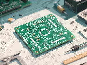
Advanced Uses of PCB Silkscreen in PCB Design
Printed Circuit Board (PCB) silkscreen is an essential and multifaceted element in modern electronics design and manufacturing. It refers to the layer of non-conductive ink
These brands already trust us.











We can delivery fast PCB Layout work as quick as 2 hours.
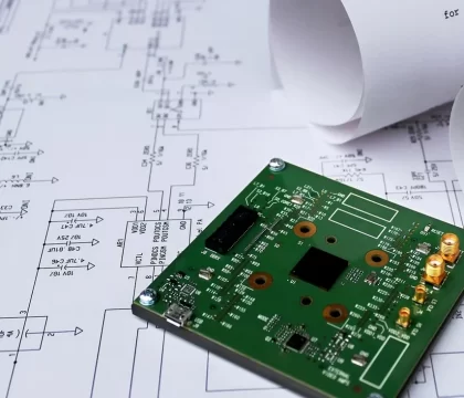
Absolutely professional PCB layout work in Altium, KiCad and Cadence output.
Delivery high reliability PCB layout work upon on our 20+ years of experience team.

RockPCB, the Division of WELLER, is a technology-based team has been a trusted provider of exceptional PCB (printed circuit board) layout services for a variety of industries. From the initial stages of schematic capture, PCB layout, our team collaborates closely with clients and board manufacturers to ensure that the final product aligns perfectly with customers’ specifications, offering a smooth and effective path to product integration. Our experienced engineering team allows us to have the capability of providing reliable and fast PCB layout solutions for complex projects, such as: controlled impedance routing (±5% tolerance), High-speed & signal integrity-sensitive designs, High-power/current layouts (up to 100A), HDI designs with micro-via (3+ mil laser drills), rapid prototyping (24-hour turnaround available), design improvements, manufacturing optimization, and quick time-to-market. The schematic capture & PCB design software we commonly use is Altium, KiCad and Cadence.
Our capabilities extend beyond just PCB layout; we also excel in PCB prototype and mass production manufacturing, components sourcing, PCB assembly, firmware burning-in, functional test, PCB reverse engineering and reworking existing PCBAs.
We can deliver PCB layout work packages as quick as 2 hours
We can support fast turn PCB prototypes as quick as 24 hours for designer for a timely verification.
All turnkey PCB assemblies made in house without any subcontract, time saving and quality to be properly controlled.
Knowledgeable, responsible partner. From PCB layout to final circuit board assembly and testing, building your product accurately and on time.
Best PCB layout in the industry. Unparalleled craftsmanship and attention to detail. PCB layout & manufacturing in the same facility.
We deliver to your schedule requirements. Our flexibility allows us to be responsive to your changing requirements.
Competitive price for Printed Circuit Boards layout, PCB fabrication and SMT assembly that brings excellent value.
Industry experience and quality is second to none.
Work with us seamlessly: Upload your design, receive a DFM review, confirm your quote, and start PCB layout. Get updates at every step for quality, cost-effective results.
01
Submit “BOM+Schematic drawing+CAD drawing+specific notes”files to our team. We will assess the design for an evaluation.
02
Our engineering and purchase team conduct a basic review to avoid obsolete components, improve manufacturability, quality, or cost-effectiveness.
03
Confirm the quote which reflects the design, lead time, and related submitting files.
04
Layout begins and you will be informed about the working progress or any issues.

From HDI to high-speed boards, we handle it all. 2000+ complex layouts delivered since 2018

Comprehensive services from consultation to production launch.

PCB layout work that are optimized for both functionality and manufacturability.

IPC-2581, Altium & Cadence Certified Professionals

30% faster cycle times vs. industry average.

Printed Circuit Board (PCB) silkscreen is an essential and multifaceted element in modern electronics design and manufacturing. It refers to the layer of non-conductive ink
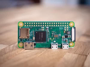
An-embedded-IoT-microcontroller-board Internet of Things (IoT) is transforming sectors from consumer goods to healthcare and agriculture, making Printed Circuit Board (PCB) design for these devices increasingly
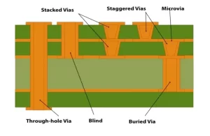
The-illustration-of-high-density-PCB-holes-structures The industrial applications of printed circuit boards continue to increase across various sectors. The ever-growing need for smaller, faster, and more feature-rich electronic devices
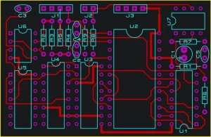
The Best Design for Manufacturing (DFM) Practices for Cost-Effective PCB Fabrication Printed Circuit Boards (PCBs) are everywhere around us. Regardless of the industry types, they
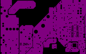
Ground and Power planes are large copper areas on the PCB that are engineered, designed, and placed to provide a stable return path for electrical
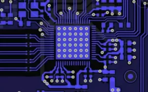
Working with electronics is a journey, and in this journey, we all start with basic electronics with bread boards and perfboards and venture our way
201, Block S, Hengyu, Science&Technology Park, No.1 Ruiji Rd, Nanlian Community, Longgang District, Shenzhen, China.
+86 755 8487 1176

At RockPCB, LLC. we strive to be your premier partner in technological design engineering, offering comprehensive solutions from circuit board design and layout to software and firmware development. Our mission is to provide applicable, intelligent solutions that propel our clients’ technologies forward.