PCB Design Optimization for Compact and Connected IoT Devices
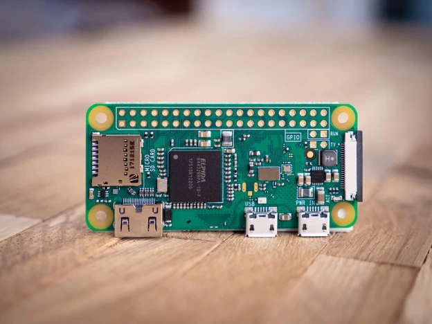
An-embedded-IoT-microcontroller-board Internet of Things (IoT) is transforming sectors from consumer goods to healthcare and agriculture, making Printed Circuit Board (PCB) design for these devices increasingly vital. At the core of IoT’s revolutionary potential lies seamless wireless data exchange, a function fundamentally reliant on the PCB. This intricate communication between interconnected devices requires a strong, reliable […]