Working with electronics is a journey, and in this journey, we all start with basic electronics with bread boards and perfboards and venture our way to a complete PCB. Don’t get me wrong, breadboards and perfboards are a great way to start your electronic journey, but a PCB is a must when working with a large project.
So in this article, we will learn all the basic aspects of a PCB design, including Schematic design, layout design, and preparing it for manufacturing. We will also talk about some of the basic tips and tricks that we always use to get many things done very easily.
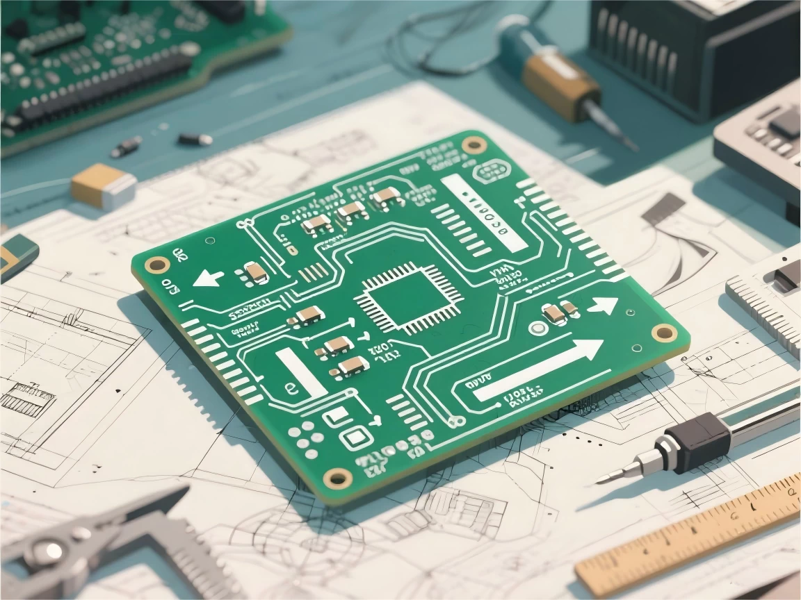
The Basics of Starting a New PCB Design
The basis of PCB design follows a standard workflow break that workflow and you will get burned. This has happened to me time and time again. It’s the most basic thing, but it’s the most important thing to consider.
The standard workflow of a PCB design focuses on first engineering and design, then creating the schematic, and finally the PCB layout for manufacturing.
As a PCB design engineer, I made numerous mistakes over the years and learned the hard way that, when the design is complex, you can test the most complicated part of the circuit on a piece of perfboard or breadboard to check if you are getting the intended output. Similarly, you can color-code your PCB for each revision; that way, you can easily remember which PCB it was when you have to refer to it in the future for another project.
In conclusion, the most important thing is to get the engineering design. Then, you can move on to the schematic and layout, and you can set standards to make the process as error-free as possible. As PCB design engineers, we always have to remember that there is no backspace in our lives.
Understanding Requirnemrs
Before you start with anything, you need to understand the requirements. Let’s say you are designing an ESP32 board for an industrial environment, then you have to consider a wide temperature range and a good protection circuit to safeguard the ESP from any external EMI, EMF, and many other things. Sounds complicated, right? But it’s not.
Consider using search engines like Auctaprts, LCSC, and DigiKey to find a specific part. For example, if you are looking for input protection ICs, there is a wide list of ICs that come with this feature. Once you choose your part, it will have a reference schematic you can start from there and make a small prototype for that part only.
Start With a Schematic
Once you have a complete understanding of the design and features you want to include, you can start designing your Schematics. First, you need to create the schematic, and then from the schematic, you will create your PCB. This is the norm for all professional PCB design software.
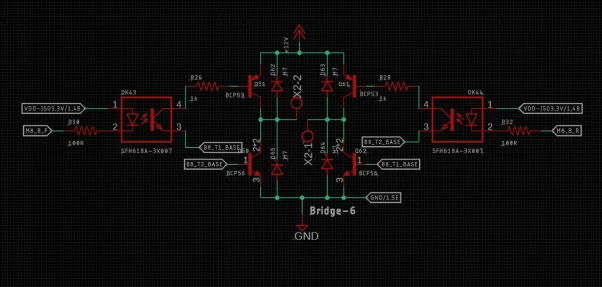
Before designing a PCB, it’s important to create a circuit schematic. This acts as a blueprint for placing components and routing traces. Most PCB design tools can import footprints and connections directly from the schematic, streamlining the layout process.
One issue you will face is that the standard libraries of any PCB design software do not include all the parts you are working with. Therefore, you can always refer to SnapEDA and grab your parts from there. Once you are done, you can get started with your schematic design. Once you are done with the schematic, you need to check for errors, You can do that with an ERC or error rule check, which is a standard feature of any design software.
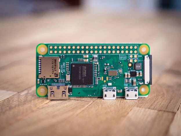
When I started, I started with Eagle PCB design software, you know why that that? It is because of SparkFun. As Sperkfun is open source, they provided the schematic and board files for every board. If you start from there, you are learning from one of the best in the industry, and that’s how I landed my first job as a PCB designer.
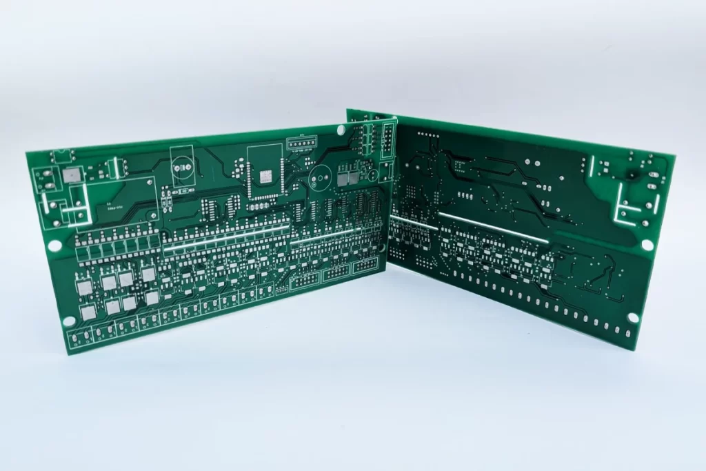
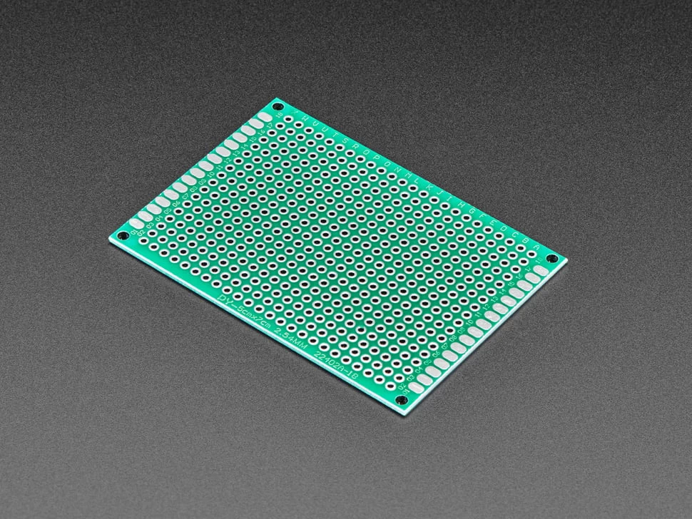
What is a PCB and How its Made?
If you are a beginner, you may have the question, What is a PCB and how is it made?
A PCB is like a layered sandwich, made up of different materials fused with heat and adhesive to form a single unit. The image below clarifies all that.
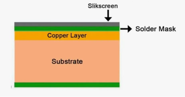
Generally, a standard double-sided PCB will have a FR4 base material or substrate, top and bottom copper layers, then we will have a solder mask and a silk screen. And that is a PCB for you. In this section, we will talk about that.
FR4 (Substrate or base material)
The core material of most PCBs is fiberglass, known as FR4, which gives the board strength and rigidity. Common thickness is 1.6mm, though some boards like LilyPad or Pro Micro use 0.8mm. Nowadays, PCB manufacturers have the option to set their own thickness, which helps in antenna-related designs.
There are other types of PCB available on the market known as Flexible PCBs use high-temp plastic like Kapton. Cheaper boards and perf boards use epoxy or phenolic materials—less durable, cheaper, and emit a bad smell when soldered. Phenolics also burn or delaminate easily under heat.
Copper Layer
A thin copper foil is added to one or both sides of the board. Most budget boards have copper on one side, while double-sided boards have it on both. The number of copper layers can range from 1 to 16 or more. Copper thickness is usually 1 oz/ft² (about 35μm), but high-power boards may use 2–3 oz.
Exposed Copper
Some areas of copper are left uncovered for soldering. These are usually pads and rings where components connect.
Soldermask
This insulating layer goes over the copper, preventing short circuits and guiding soldering. It’s typically green, but can be red, white, purple, or other colors.
Silkscreen
The top printed layer shows labels, symbols, and text to help identify pins and parts. It’s usually white but can be in other colors too.
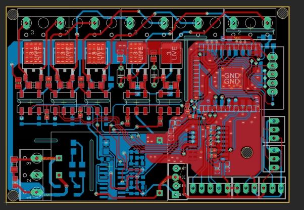
Designing your PCB
Now, you can start designing your own PCB, but before you design your PCB, you need to set your DRC. Which is one of the most important steps in your PCB design!

DRC stands for Design Rules Check, and it simply checks for any form of erosion that is present or will come with designing your PCB. Every manufacturer will have their own limitations, you have to first decide on a PCB manufacturer and then from there capabilities page, you can set the value for your DRC.
With DRC (Design Rule Check), you need to define parameters such as wire, pad, and via clearance. You also have to specify the minimum trace width, minimum drill diameter, microvia diameter, annular ring size, thermal isolation, and other critical layout constraints.
If I have confused you with all the above unknown terminology, let me go through it one by one.
- Wire Clearance – refers to the minimum spacing between copper traces to prevent short circuits.
- Pad Clearance – is the minimum distance between a pad and other elements like traces or vias, helping avoid solder bridging.
- Via Clearance – ensures there’s enough space between vias and surrounding copper to prevent shorts. The minimum trace width defines how narrow a copper trace can be, which directly affects its ability to carry current safely.
- Minimum Drill Diameter – is the smallest hole size a manufacturer can reliably drill.
- Microvia diameter – applies to high-density designs, indicating the size of very small vias used to connect layers in compact PCBs.
- The Annular Ring – The annular ring is the ring of copper around a drilled hole, necessary for solid connections and mechanical strength.
- Thermal Isolation – refers to the spacing around thermal relief pads, which balances effective heat dissipation with ease of soldering during assembly.
Each of these parameters must be carefully set during DRC to ensure the PCB functions correctly and can be manufactured without issues.
Some Design Norms Before Manufacturing
There are some basic design norms and some rules of thumb that we follow during our PCB design, which make things so much easier and simpler.
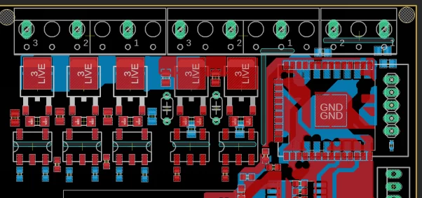
Use a Ground Plane
Every PCB needs a clear ground connection to ensure a good ground connection between all the components. The easiest and most reliable way to do this is by using a ground plane, a full layer of copper dedicated to ground. Not only that a good ground connection, it also reduces Electro Magnetic Interferences (EMI).
Surprisingly, many beginners skip this step, which leads to noise issues in both digital and analog circuits. In most modern designs, a solid ground plane is standard. While techniques like split or star grounds exist, they’re only suited for specific cases, not typical designs.
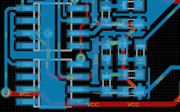
Place all Components Before Routing
Once you have made a ground plane, you can start laying your components to the specific spot where it will be easier to route traces with it. Don’t begin routing until placement is done, or you’ll likely have to redo it.
Try to place parts so wires don’t cross too much. When you start routing, keep traces short and direct, avoid too many layer changes, use as few signal layers as possible, and always include a solid ground plane to reduce noise. These steps help make your PCB work better and are useful in almost all types of designs.
Use Via Stitching
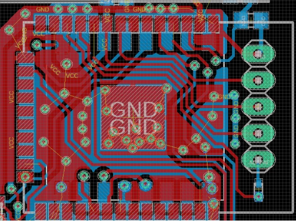
Via stitching is a technique where multiple vias are placed around a PCB, usually connecting ground planes on different layers. This helps reduce noise, improve EMI performance, and create a stronger ground connection. It’s especially useful near high-speed signals, power areas, or around board edges for shielding.
Placing Decoupling Capacitors close to a IC
Decoupling capacitors should be placed as close as possible to an IC’s power pins. This helps filter out noise and provides a stable power supply to the chip during fast switching. The closer the capacitor is, the more effective it is at reducing voltage dips and high-frequency noise.
All in all, following standard PCB design practices and tried-and-true rules of thumb like keeping traces short, using a solid ground plane, placing decoupling capacitors close to ICs, and maintaining proper clearance can save you from headaches later. These simple habits help ensure your board works reliably and is easier to manufacture.
Few Finishers!
Now your job is done, right? Not so quick, once your PCB layout is complete, you still need to generate the manufacturing files. Most PCB software can do this automatically, but it’s important to review the files carefully to make sure all settings are correct before sending them to the manufacturer.
You also need to set the silk screen text size and many other parameters to ensure all the components have levels beside them. This is not a mandatory step, and many modern-day complex PCBs, all in all, remove the part marking, but if you are building a prototype PCB and soldering it by hand, this is a completely necessary step.
After generating the manufacturing files, always take time to review them. Check that all layers, drill files, and design settings are correct. A quick review can catch issues that might cause delays or errors during production.
Congrats, you’ve finished the design! Now the manufacturer will review it to check if it meets their production limits. If it passes the DFM check, your PCB moves on to fabrication and assembly.
Contact us freely if you have any questions on your new PCB design.