Printed Circuit Board (PCB) silkscreen is an essential and multifaceted element in modern electronics design and manufacturing. It refers to the layer of non-conductive ink printed on the surface of a PCB that provides text, symbols, component markings, and other critical information.
While traditionally associated with simple component labeling to aid PCB assembly and troubleshooting, PCB silkscreen has evolved into an advanced and versatile tool that significantly enhances PCB functionality, aesthetics, and manufacturability. This article explores the advanced uses of PCB silkscreen, articulated in a manner accessible to students and businesses considering PCB orders.
Understanding PCB Silkscreen
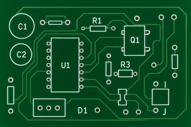
PCB silkscreen acts much like a map or legend for electrical circuits. It identifies components, test points, polarity markers, warnings, logos, and version numbers. This visual information is vital for assembly line workers, engineers, and technicians during manufacturing and maintenance.
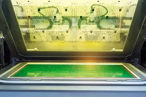
The silkscreen ink is typically an epoxy-based, non-conductive material, commonly available in white, black, or yellow colors, to provide high contrast on standard PCB substrates. The layer is printed using techniques like manual screen printing, Liquid Photo Imaging (LPI), and Direct Legend Printing (DLP), each with varying precision, cost, and production suitability.
Advanced Functional Uses of PCB Silkscreen
Advanced functional uses of PCB silkscreen go well beyond simple component labeling, evolving into several critical roles that enhance PCB design, assembly, testing, and maintenance. These advanced functions improve the accuracy, efficiency, and reliability of PCB manufacturing and usage:
Facilitating Accurate Component Placement and Orientation
Advanced silkscreens provide detailed and clear markings such as component reference designators (e.g., R1, C2), polarity indicators (+ or - signs for capacitors and diodes), and pin-1 markers on integrated circuits. These markings serve as precise guides during assembly, significantly reducing errors like reversed or misplaced components, which could cause circuit failure. For instance, polarized components like electrolytic capacitors or diodes must be oriented correctly, and silkscreen symbols ensure this happens without confusion.
Layer Management and Multi-Layer Board Visibility
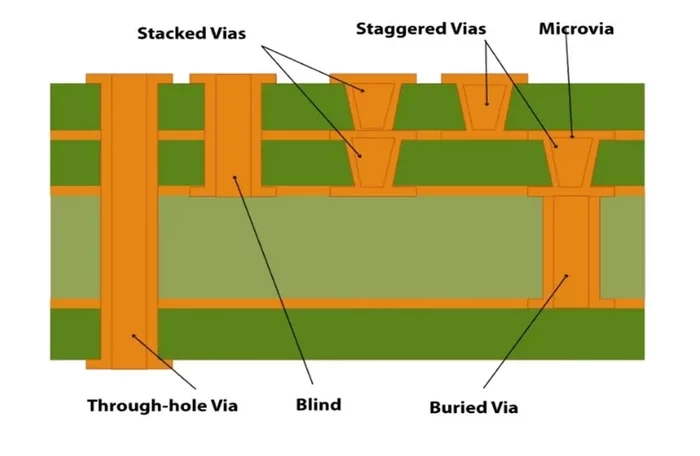
In complex multi-layer PCBs, many circuit traces and components are stacked in layers that are not visible from the top surface. Silkscreen layers help manage and identify these layers by marking layer edges, test points, or signal zones related to specific layers. This is especially important for high-density interconnect (HDI) boards where compact layouts demand precise visual cues to avoid mistakes such as short circuits or misplaced parts. Silkscreen acts as a roadmap and helps maintain clarity across complicated layered designs. Suggested Reading:
Avoid PCB Fab Errors: Why Your Fabrication Drawing is Critical
Multi-Color Silkscreen for Functional Zoning
Modern PCB manufacturing often incorporates multi-color silkscreens to quickly differentiate between functional zones or types of components. For example, power circuits might be marked in blue, signal paths in red, and ground planes in another color. This use of color coding enhances assembly speed and debugging efficiency, particularly in complex or densely populated boards. It also allows better grouping of components and visual distinction, which supports quality control.
Troubleshooting and Maintenance Enhancement
Silkscreen markings include not just component IDs but also test points, jumper settings, revision/version numbers, and manufacturing batch codes. These markings help service technicians rapidly identify critical nodes for testing without needing detailed schematics on hand. They also enable efficient tracking of PCB revisions and quality control batches, which is crucial for post-production support, repair, and warranty management. Suggested Reading:
Anti-Counterfeiting and Security Measures
Some advanced silkscreens incorporate unique security features like serial numbers, QR codes, or special cryptic markings embedded subtly in the silkscreen layer. These identifiers help in authenticating the PCB as a genuine product and prevent illicit duplication or counterfeiting. Such features are especially valuable in high-reliability or proprietary technology devices where intellectual property protection is critical.
Branding and Enhanced Aesthetic Value
Beyond practical functionality, silkscreens contribute to the professional look and brand identity of electronic products. Custom logos, stylized fonts, corporate colors, and decorative patterns printed on the PCB surface make the product appear more polished and trustworthy. This is important for consumer-facing products where visual impression matters.
Durability and Manufacturing Optimization
Advanced silkscreens use UV-curable and chemically resistant inks that withstand high-temperature soldering processes and wear, ensuring longevity of the markings throughout the lifecycle of the PCB.

The use of precise printing methods like Liquid Photo Imaging (LPI) or Direct Legend Printing (DLP) ensures high resolution and alignment precision, reducing manufacturing defects and aiding in automated optical inspection (AOI).
Design Considerations for Advanced Uses of PCB Silkscreen
Advanced design considerations for PCB silkscreen are critical to ensure clear communication, manufacturability, durability, and functionality of the printed markings on circuit boards. These considerations balance legibility, placement, color contrast, manufacturing constraints, and compliance with industry standards.
The following table provides a comprehensive summary of the design considerations for PCB silkscreen:
Category
Details
Purpose
Font Size
Minimum 0.035 inches (0.89 mm), preferred 0.050 inches (1.27 mm), larger (~0.080 inches) for logos
Ensures readability by assembly technicians and clarity
Line Width
Minimum 0.006 inches (0.15 mm), adjustable per font size and printer capability
Prevents smudging and maintains clean ink prints
Font Style
Simple sans-serif fonts like Arial or Helvetica for distortion-free printing
Avoids distortion and preserves legibility
Spacing and Placement
Min. 0.006 inches (0.15 mm) clearance from pads; no printing on pads and via; strategic placement to avoid overlap
Prevents overlap and ink interference during soldering
Color and Contrast
White on green masks (high contrast), black on light masks; avoid pink and other poor adhesion colors
Enhances visibility and inspection accuracy
Material and Ink
Non-conductive epoxy-based inks, UV-curable preferred for durability and fast curing
Ensures durability through heat and chemical exposure
Industry Standards
Follow IPC-A-600, IPC-2221, IPC-7351; include regulatory symbols legibly
Compliance with industry and regulatory requirements
Manufacturing Optimization
Prioritize critical markings, avoid overcrowding; clear symbols for AOI and human use; print on one or both sides as needed
Facilitates assembly and automated inspection
Resolution and Printing
Screen printing for general use; LPI/DLP for finer details; maintain font width-to-height ratio ~1:6
Balances detail and efficiency based on design complexity
Additional Considerations
Avoid overlaps; clearly mark test points, jumper settings; include version numbers and batch codes
Supports maintenance, traceability, and quality control
These design factors collectively ensure that the PCB silkscreen layer effectively communicates vital information, supports assembly and troubleshooting, enhances product quality and traceability, and meets manufacturing capabilities and standards.
Manufacturing Implications and Cost Efficiency
Choosing the right silkscreen method impacts both cost and quality. Manual screen printing is suitable for prototypes and small runs, but lacks precision, while LPI offers finer detail for medium to high volumes.
DLP excels at customization and detailed prints, but is costlier. Strategic use of silkscreen, such as limiting printing to only one PCB side or using standard colors, can reduce manufacturing costs by up to 5% without sacrificing functionality.
Conclusion
PCB silkscreen has transcended its original role as mere labeling to become an indispensable, multi-functional layer in PCB design. It enhances assembly accuracy, facilitates troubleshooting, improves product branding, and bolsters intellectual property protection.
Advanced silkscreen applications, including multi-color printing and unique identifiers, reflect the increasing complexity and quality demands of modern electronics. For students and businesses, understanding these advanced uses aids in appreciating PCB design intricacies and making informed decisions when ordering or designing printed circuit boards.
FAQs
1. What is PCB silkscreen and why is it important?
PCB silkscreen is the layer of non-conductive ink printed on a printed circuit board that provides component labels, symbols, logos, test points, and other important information. It is essential for accurate assembly, troubleshooting, and product identification.
2. What colors are typically used for PCB silkscreen?
The most common silkscreen colors are white and black due to their high contrast with standard green, yellow, or white solder masks. Other colors like red, blue, and yellow are also sometimes used for functional zoning or branding, but pink is generally not recommended due to manufacturing challenges.
3. What are the common methods for applying PCB silkscreen?
The main silkscreen printing methods include manual screen printing, Liquid Photo Imaging (LPI), and Direct Legend Printing (DLP). Manual screen printing is suitable for low volume or prototypes, LPI offers high precision for medium to high volume, and DLP is ideal for detailed, customizable prints, especially in small runs.
4. What design considerations ensure a high-quality silkscreen layer?
Key design factors include using a minimum font size of about 0.035 inches (0.89 mm), maintaining line widths of at least 0.006 inches (0.15 mm), proper spacing from solder pads and vias, selecting high-contrast colors, and using simple fonts like Arial or Helvetica to maximize legibility and prevent smudging during manufacturing.
5. Can PCB silkscreen improve security and branding?
Yes. Advanced silkscreens can include unique identifiers such as serial numbers, QR codes, or cryptic markings to help prevent counterfeiting. Additionally, custom logos, colors, and decorative patterns can enhance the visual appeal and professional branding of the final product.
References
1. The Ultimate Guide to PCB Silkscreen: Techniques, Materials, and Best Practices – WELLERPCB
2. PCB Silkscreen: What is it? – Wevolver
3. Comprehensive Guide to PCB Silkscreen – Sierra Circuits
4. PCB Silkscreen: All You Need to Know – Altium
5. Essential PCB Silkscreen Guidelines for Layout- Cadence
6. Legend Print – Eurocircuits


