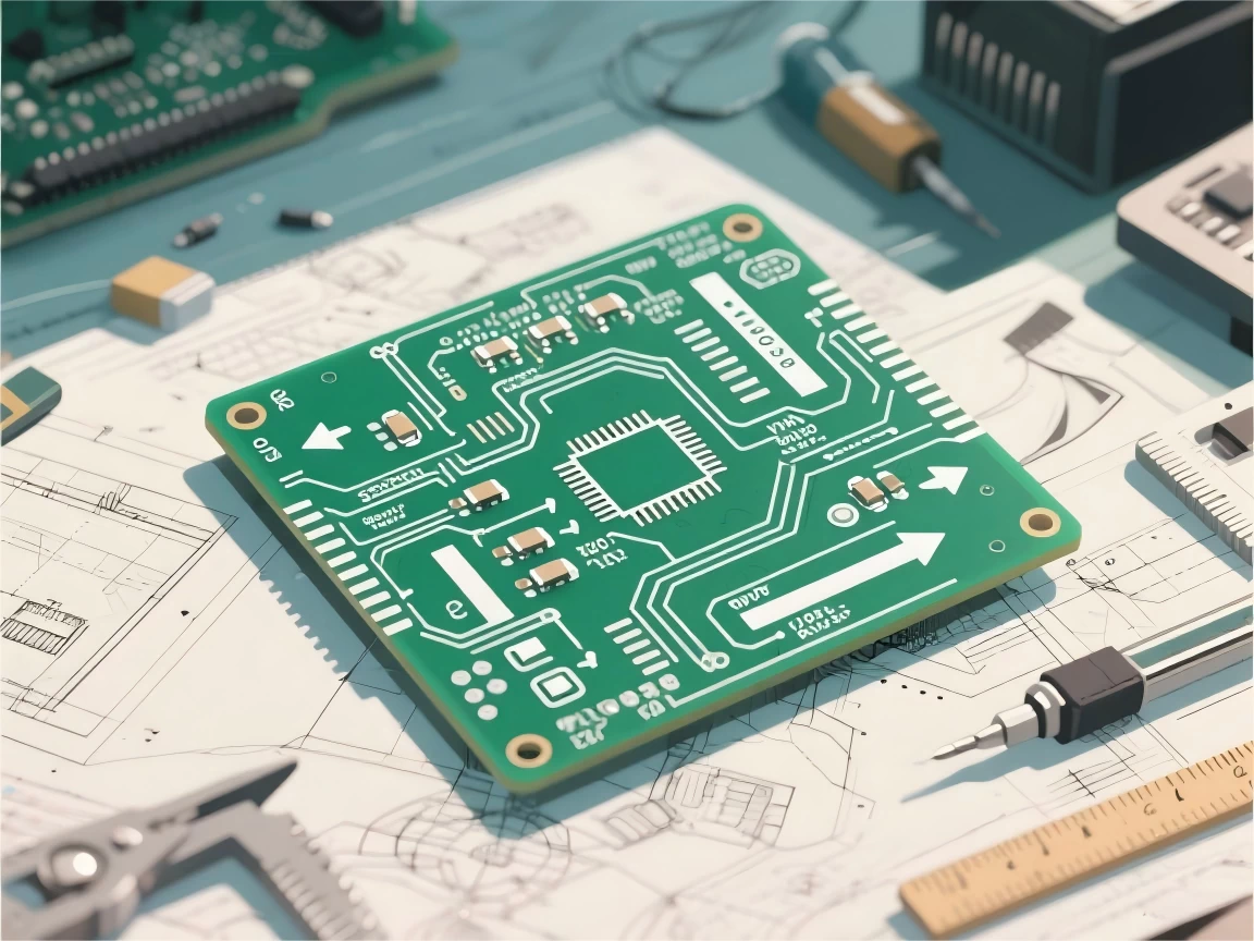
The industrial applications of printed circuit boards continue to increase across various sectors. The ever-growing need for smaller, faster, and more feature-rich electronic devices means that traditional PCB designs’ interconnect methods must continue to evolve.
As miniaturization is one of the key aspirations for modern electronic gadgets, the demand for higher component density and improved signal integrity brings about innovative solutions for layer-to-layer connections. Among these advanced technologies, blind and buried vias are crucial enablers for high-density interconnect (HDI) PCBs.
These specialized via types offer significant advantages over conventional through-hole vias by providing selective layer connectivity, thereby unlocking valuable routing space and enhancing electrical performance in complex designs.
In this article, we will look into the essential details about blind and buried vias, exploring their fundamental principles and how they facilitate advanced PCB designs. We will discuss the creation techniques, benefits, and related design considerations to help engineers and designers choose effectively between the two via types.
What are Vias?
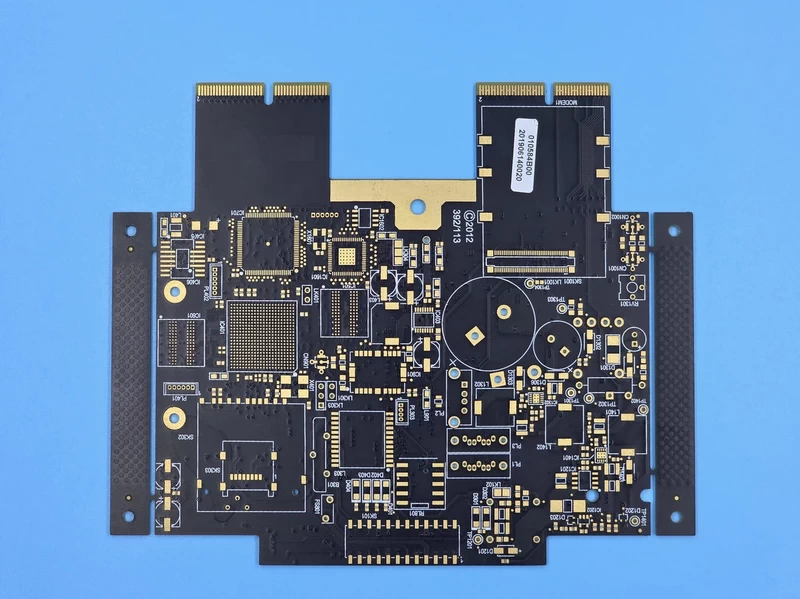
In multi-layer PCBs, different layers must be connected through vertical connectors. These connections prevent the need for any external connectors, thereby reducing the PCB size and increasing component density. Such vertical connectors are called vias. Essentially, vias are conductive barrels drilled across layers, providing electrical connectivity.
Role of Vias
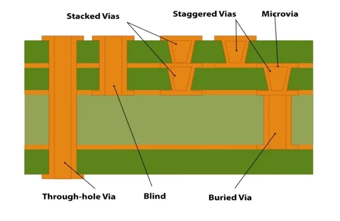
The role of a via is to establish a layer-to-layer electrical conductivity in a PCB. Based on the type of connection and position of layers, we divide vias into three types:
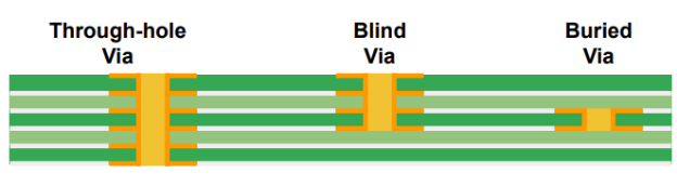
- Through-hole Vias - Penetrate through the PCB to connect the outermost layers. These vias pass through all the intermediate layers.
- Blind Vias - Connect the outermost layer to one or more internal PCB layers, without penetrating to the other side.
- Buried Vias - Connect two or more inner layers of the PCB without any connection to the outer layers. They are usually invisible from the outside of the PCB.
What are Blind Vias?
Blind Vias connect the outer layer of a multilayer PCB to one or more internal layers. These via types don’t penetrate through, so they are only visible from one side of the board; hence, they’re called ‘blind’ vias. Due to vertical connections with multiple layers, blind vias reduce board size, contributing to more compact PCBs and improved signal integrity.
During PCB fabrication, blind vias are drilled through the surface, extending to a specific portion of the board. Not only do they reduce board size, but also minimize the necessary layers for routing.
What are Buried Vias?
Buried Vias connect two or more internal layers of a PCB. They are not connected to any outer layer. So, they are completely hidden inside a PCB. The isolation from the outer layers enables designers to use the surface for mounting SMT components, which directly contributes to board miniaturization. Likewise, it facilitates routing on surface layers without hindering any electrical paths.
Similar to blind vias, the buried vias also help improve component density and can facilitate routing complexity in smaller circuit boards. They are an essential feature of a multilayer PCB, but require additional fabrication steps such as:
- Drilling
- Lamination
Hence, buried vias are generally costlier than through-holes and blind vias.
How are Blind and Buried Vias Created?
Vias are created either before or after the multi-layer lamination process. They are added to the PCB through drilling techniques, which require high precision and accuracy.
Blind Via Creation
There are two steps in creating a blind via:
- Drilling - The holes are drilled with a mechanical or laser drill from the outside to a specific depth. The drilling depth is one of the most critical features. Too deep or shallow holes can lead to incorrect electrical connections.
- Plating - Once drilling is completed, the holes are copper-plated to establish an electrical connection between the layers.
Suggested Reading: The Importance of Copper Pouring In Copper-Free Areas While Creating PCBs.
Buried Via Creation
Buried vias require a few additional steps because of the layer positioning. Here is a quick look:
- Drilling - Vias are drilled through the designated inner layers that need interconnection.
- Plating - Once drilling is completed, the holes are copper-plated to establish an electrical connection between the layers.
- Plating - The drilled holes are plated with copper, creating conductive pathways between these inner layers.
- Lamination - The processed and drilled inner layers, along with prepreg material and outer copper foils, are stacked and laminated together under heat and pressure to form the complete multilayer PCB. The buried vias are now internal and not accessible from the outer surfaces.
The IPC-221B manual provides clear guidelines for creating buried and blind vias. Engineers and designers refer to these guidelines for professional and compliant PCB designs in the industrial sector.
Recommended Reading: The Difference between IPC-6012, IPC-A-600, and IPC-A-610
Benefits of Blind and Buried Vias
Blind and buried vias facilitate high-density PCB designs. They help in achieving complex layer-to-layer connections, reduced layer count, increased signal integrity, and reduced crosstalk. Hence, wearable gadgets, smartphones, and miniaturized electronic devices are some of the common examples of their applications.
While blind and buried vias may differ in design and fabrication, their benefits are quite similar and overlap in most cases. Here is a quick look at some of the major benefits of blind and buried vias.
Enhanced Component Density
Blind and buried vias are essential for achieving high component density in modern PCBs. By creating connections between surface components and inner layers, blind vias allow for complex interconnections within a smaller footprint. Likewise, buried vias facilitate SMT device mounting circuit as they don’t directly interact with the outermost layers of the PCB. This efficient use of board space directly contributes to a reduction in the overall size and weight of the final electronic product.
Improved Routing Density
Just like the component density, blind and buried vias improve the routing density as the holes eliminate the need for through-hole passages and can take alternative routes to pass a signal. It directly contributes to the reduced board size.
Better Signal Integrity in High-Frequency Designs
Blind and buried vias enhance signal integrity in high-frequency applications by confining signals to specific layers. So, it minimizes electromagnetic interference and crosstalk between adjacent traces. This focused signal routing over vias leads to cleaner transmission paths, ultimately improving overall signal quality and the reliability of high-speed electronic devices.
Multilayer Design Support
For complex multilayer PCBs, blind and buried vias provide a crucial alternative to space-consuming through-hole vias. They establish efficient and reliable interconnections between specific layers, improving signal integrity and enabling the intricate routing required for sophisticated circuitry and dense component integration.
Suggested Reading: Multi-layer PCB Stack-up Design Guideline
Cost Considerations
Fabrication cost is one of the differentiating factors between blind and buried vias. Blind vias help reduce the board size which directly impacts the fabrication cost. The overall size, and weight of the products reduces which plays a pivotal role in cost management especially while producing large PCB batches.
On the other hand, buried vias follow a similar fabrication process, but the overall cost is increased due to additional drilling and lamination steps. As a result, buried vias cost more than blind vias.
Key Differences Between Blind and Buried Vias
Blind and buried vias serve a similar purpose i.e., to route signals from within the PCB. However, there are some key differences between the two types, highlighted in the table below.
| Feature | Blind Via | Buried Via |
|---|---|---|
Outer Layer Connection | 100% connection to at least one outer surface. | 0% connection to either outer layer. |
Manufacturing Timing | Drilled and plated on inner layer cores before outer layers are laminated. This often occurs early in the sequential lamination process for multi-layer boards. | |
Routing Space Impact (Outer Layers) | Can potentially free up 30-50% of routing space on inner layers compared to through-hole vias, but the landing pad still occupies space on the connected outer layer. | Leaves 100% of both outer layers free from via obstructions, maximizing space for component placement and routing. |
Routing Space Impact (Inner Layers) | Improves routing density on inner layers by allowing layer-specific connections, potentially increasing routing channels by 20-40% on those layers involved in the blind via connection. | |
Signal Integrity | Reduces via stub length significantly (e.g., a blind via connecting 2 layers in a 6-layer board has a stub of ~67% less than a through-hole via if the signal travels only between those 2 layers), improving signal rise times and reducing reflections at higher frequencies (e.g., >1 GHz). | Offers the shortest possible interconnect paths between inner layers (stub length is effectively zero for the connected layers), minimizing signal distortion and EMI, crucial for very high-speed signals (e.g., >5-10 GHz). |
Accessibility for Rework/Testing | More accessible than buried vias as one end is on an outer layer, allowing for easier probing and potential rework. | Less accessible for rework or testing as they are entirely internal to the PCB. Specialized techniques like micro-probing might be required. |
Manufacturing Complexity | Generally involves one or more additional drilling and plating steps compared to standard through-hole processing. Aspect ratios (depth-to-diameter) are critical (e.g., typically aim for 10:1 or less for reliable plating). | Requires at least one extra lamination cycle and precise registration between inner layers. Aspect ratios for buried vias also need careful control. |
Cost | Typically increases PCB cost by 15-30% compared to boards with only through-hole vias, depending on the number and complexity of blind vias. | Generally increases PCB cost by 25-50% or more compared to standard through-hole boards due to the added lamination cycles and processing. |
Layer Stackup Planning | Requires careful consideration of the sequential build-up and the depth of the blind via to ensure reliable drilling and plating within the specified layers. | Demands meticulous planning of inner layer connections and the sequence of lamination to correctly form the buried vias before outer layer processing. |
Common Applications | Smartphones (dense interconnects for tightly packed components), tablets, HDI boards (e.g., with trace widths/spaces of < 75 µm), where space saving on inner layers connected to the surface is crucial. | High-performance computing (complex internal signal routing), advanced networking equipment (high layer counts, e.g., > 8 layers), multi-layer boards with dense internal signal layers requiring minimal surface obstruction. |
Design Considerations for Buried and Blind Vias
Designing with buried and blind vias demands careful considerations such as.
- Maintaining signal integrity requires careful planning of via placement and routing, particularly for high-speed signals, to avoid impedance discontinuities and reflections.
- The layer stackup design must strategically accommodate these vias, considering the number and arrangement of layers and their impact on impedance control.
- Thermal management becomes crucial as these internal vias can affect heat dissipation, necessitating adequate thermal relief and balanced via distribution.
- Ensuring long-term reliability and durability involves assessing resistance to mechanical stress, thermal cycling, and potential via failures. Addressing these interconnected challenges is paramount for successful implementation.
Challenges in Creating Buried and Blind Vias
There are various challenges associated with buried and blind via creation, such as:
- Manufacturing limitations regarding minimum via size and aspect ratio can constrain design choices and feasibility, necessitating early consultation with fabricators.
- Testing complexity increases as these internal connections are harder to inspect, potentially impacting quality control measures.
- During assembly alignment, precise component placement over these vias is critical to avoid soldering or connection failures.
- Signal attenuation in blind vias can be a concern in high-frequency designs, requiring careful impedance matching and signal integrity analysis.
Suggested Reading: The Best Design for Manufacturing (DFM) Practices for Cost-Effective PCB Fabrication.
Conclusion
Blind and buried vias represent essential interconnect technologies for achieving the miniaturization, increased density, and enhanced electrical performance demanded by modern electronics. While their fabrication introduces complexities and design challenges concerning signal integrity, thermal management, and manufacturability, the benefits they offer in terms of routing efficiency and device form factor are often indispensable for advanced applications. Careful consideration of design rules, manufacturing capabilities, and the strategic implementation of these advanced via types are crucial for unlocking the full potential of high-density interconnect PCBs in today’s rapidly evolving technological landscape
FAQs
1. What are the main benefits of using blind and buried vias?
The primary advantages include increased routing density by freeing up space on outer and inner layers, improved signal integrity due to shorter connections and reduced stubs, and the ability to achieve smaller and lighter electronic devices. They enable more complex and compact designs that traditional through-hole vias cannot accommodate.
2. How are blind and buried vias created?
Blind vias are typically formed by controlled-depth drilling (mechanically or with lasers) after inner layer processing or during sequential lamination, followed by plating. Buried vias are created by drilling and plating inner layers before the outer layers are laminated, effectively embedding them within the board.
3. What are some of the challenges in designing with these vias?
Design challenges include ensuring signal integrity at high speeds, managing layer stackup for proper impedance control, and considering thermal management due to the internal nature of the vias. Manufacturing limitations on via size and aspect ratio, as well as increased testing complexity, also need careful attention.
4. Are PCBs with blind and buried vias more expensive?
Yes, PCBs utilizing blind and buried vias generally have a higher manufacturing cost compared to those with only through-hole vias. This is due to the additional processing steps involved in their creation, such as controlled-depth drilling, extra plating cycles, and potentially more complex lamination processes.
5. How does ECAD software aid in designing with blind and buried vias?
ECAD (Electronic Computer-Aided Design) tools allow designers to define and place blind and buried vias within the layer stackup. These tools provide features to control via depth, manage connections between specific layers, and check design rules related to via size, spacing, and aspect ratios to ensure manufacturability.
6. What considerations should be made in routing software when using these vias?
Routing software needs to be configured to understand the connectivity established by blind and buried vias, ensuring traces are appropriately routed to and from the correct layers through these internal connections. Designers must also consider the impact of via placement on signal integrity, often utilizing simulation tools integrated with the routing software to optimize via locations and trace paths.