Introduction
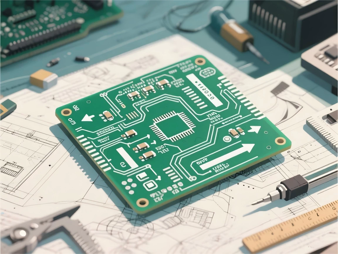
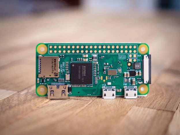
Printed Circuit Board (PCB) design is both an art and a science. A well-designed board ensures reliability, efficiency, and cost-effectiveness, while a poor PCB design can lead to signal interference, overheating, or manufacturing failures. This guide walks through some critical design considerations with visual examples to help you avoid common pitfalls.
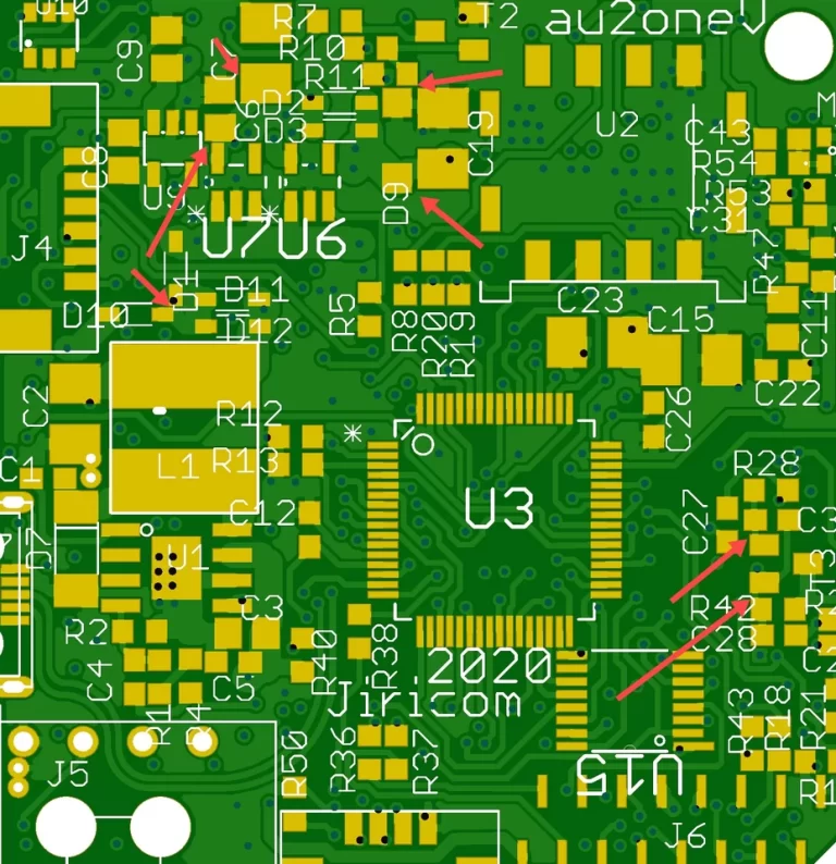
1. Poor Component Placement: The Root of Many Issues
Common Mistakes:
- Crowded Layouts: Placing components too close together makes routing difficult and increases heat buildup.
- Ignoring Signal Flow: Components should follow logical signal paths (e.g., microcontroller → connectors → sensors).
- Neglecting Thermal Management: High-power components (e.g., voltage regulators) should be placed near board edges for better heat dissipation.
How to Fix It:
- Group related components (e.g., power supply, analog, digital sections).
- Leave space for routing and cooling.
- Follow manufacturer recommendations for component spacing.
2. Inadequate Power & Ground Planes
Common Mistakes:
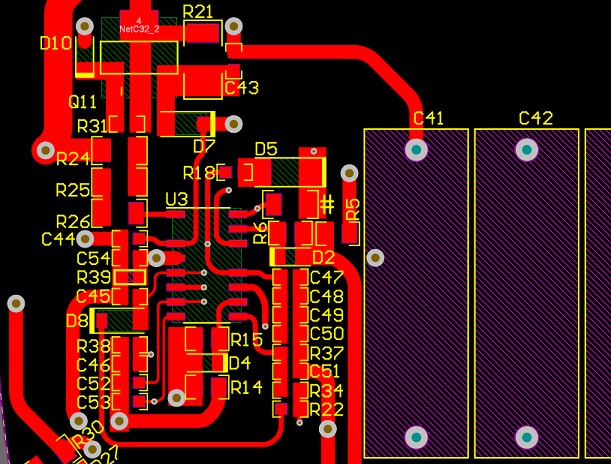
- Thin or Split Power Traces: Causes voltage drops and overheating.
- Insufficient Grounding: Leads to electromagnetic interference (EMI) and unstable signals.
- Using Grid Planes Instead of Solid Copper: Increases impedance and noise.
How to Fix It:
- Use dedicated power and ground planes (especially in multilayer PCBs).
- Avoid long, thin traces for high-current paths—use wider traces or copper pours.
- Minimize ground loops by ensuring a low-impedance return path.
3. Signal Integrity Problems
Common Mistakes:
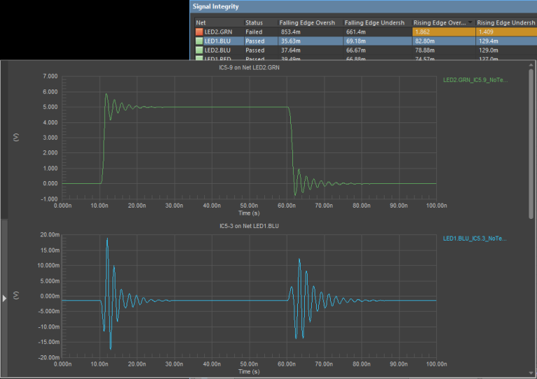
- Ignoring Trace Impedance: Causes signal reflections in high-speed designs (e.g., USB, HDMI).
- Long, Meandering Traces: Introduces delays and noise.
- Poor Differential Pair Routing: Leads to skew and signal degradation.
How to Fix It:
- Match trace lengths for high-speed signals (e.g., DDR memory, Ethernet).
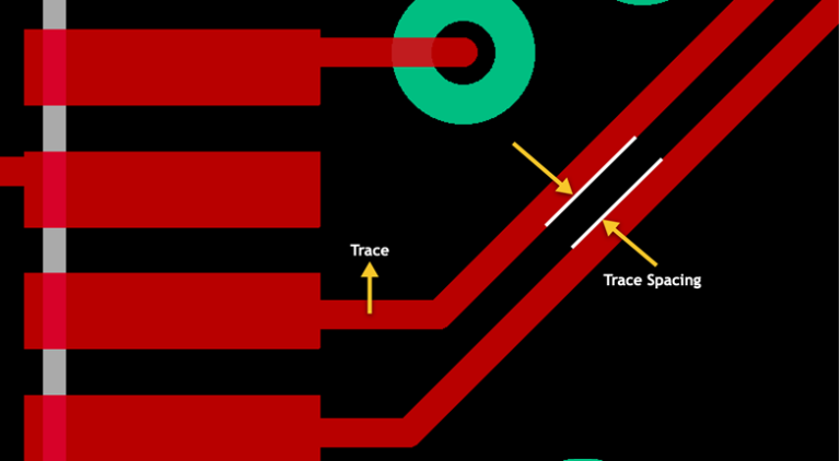
- Keep differential pairs tightly coupled with consistent spacing.
- Use 45° angles (not 90°) to reduce impedance discontinuities.
4. Overlooking Thermal Management
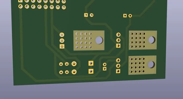
Common Mistakes:
- No Thermal Relief for Pads: Makes soldering difficult and traps heat.
- Ignoring Heat-Generating Components: Leads to premature failure. noise.
- Poor Airflow Design: Causes hotspots in enclosed devices.
How to Fix It:
- Add thermal vias under hot components (e.g., QFN, BGA packages).
- Use copper pours connected to ground planes as heat spreaders.
- Consider heatsinks or fans for high-power designs.
5. Ignoring Design for Manufacturing (DFM) Rules
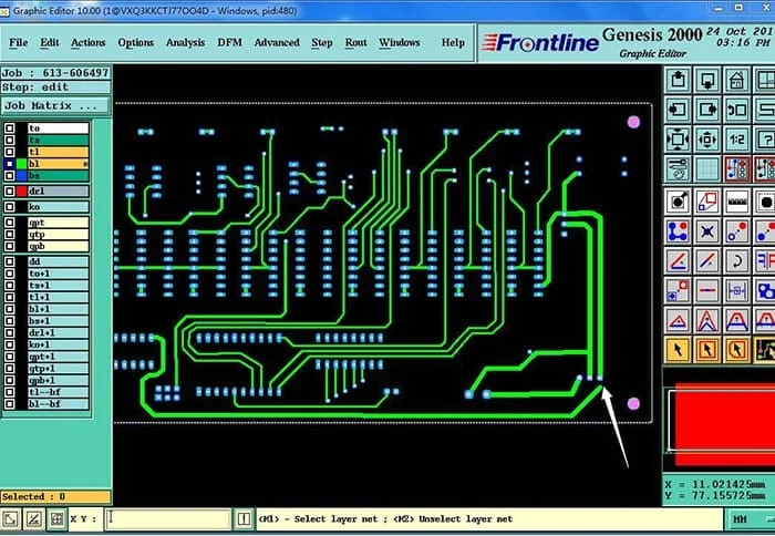
Common Mistakes:
- Too Small Traces/Vias: Can break during manufacturing.
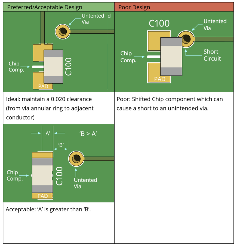
- Insufficient Clearance: Causes short circuits.
- Missing Silkscreen Labels: Makes assembly and debugging harder
How to Fix It:
- Follow your PCB manufacturer’s design rules (e.g., minimum trace width, via size).
- Run a Design Rule Check (DRC) before sending files for production.
- Label components clearly to avoid assembly errors.
6. EMI & Noise Issues
Common Mistakes:
- Unfiltered Power Lines: Introduces noise into sensitive circuits.
- Long Unshielded Traces: Acts as antennas for interference.
- Improper Grounding: Creates ground loops and EMI problems.
How to Fix It:
- Use decoupling capacitors near IC power pins.
- Keep high-speed traces away from analog signals.
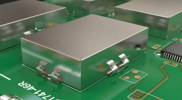
- Add shielding (e.g., grounded metal cans) for RF-sensitive circuits.
Conclusion: Design Smart, Build Right
Avoiding these common PCB design mistakes will save you time, money, and frustration. Always:
- Plan component placement carefully.
- Optimize power and ground distribution.
- Follow DFM guidelines.
- Manage heat effectively.
- Ensure signal integrity with proper routing.
- Minimize EMI risks.
By applying these best practices, you’ll create reliable, high-performance PCBs that work right the first time.
Need a PCB design review? Share your layout in the comments for expert feedback! Or contact us freely now.

