Introduction
Surface Mount Technology (SMT) has revolutionized electronics manufacturing, enabling smaller, faster, and more efficient PCB assemblies. However, poor PCB design can lead to costly SMT assembly issues, including misaligned components, solder defects, and reduced reliability.
This blog explores how PCB design decisions affect SMT assembly and provides best practices to optimize manufacturability.
1. Component Placement & Orientation
Common Issues:
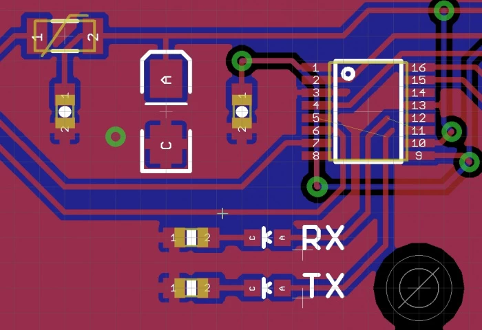
- Insufficient Spacing: Components placed too close together can cause tombstoning or solder bridging.
- Inconsistent Orientation: Mixed component angles (e.g., 0°, 90°, 45°) increase placement errors.
- Large Components Near Small Ones: Heavy parts (e.g., connectors) can shadow smaller passives during reflow.
Best Practices:
- Follow manufacturer-recommended land patterns.
- Maintain ≥0.3mm clearance between components.
- Align similar components in the same direction (0° or 90°).
2. Pad & Footprint Design
Common Issues:
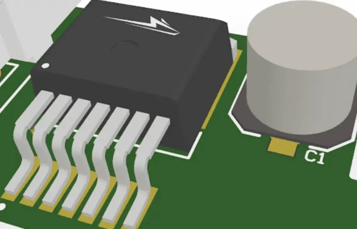
- Undersized Pads: Lead to weak solder joints or component misalignment.
- Incorrect Thermal Relief: Causes uneven heating during reflow.
- Missing Solder Mask Dams: Increases bridging risk for fine-pitch ICs (e.g., QFN, BGA).
Best Practices:
- Use IPC-7351 standards for footprint design.
- Add thermal relief for large copper pads.
- Include solder mask between pads (especially for <0.5mm pitch).
3. Solder Paste & Stencil Design

Common Issues:
- Insufficient Solder Paste: Causes open solder joints.
- Excessive Paste: Leads to bridging or component floating.
- Poor Stencil Aperture Design: Incorrect aperture ratios affect paste release.
Best Practices:
- Follow a 1:1 pad-to-aperture ratio for standard components.
- Use step stencils for mixed component sizes.
- Avoid oversized apertures for fine-pitch devices.
4. Panelization & Fiducial Marks
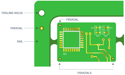
Common Issues:
- Missing Fiducials: Reduces pick-and-place machine accuracy.
- Weak Panel Breakaway Tabs: Causes board damage during depaneling.
- Incorrect Panel Spacing: Leads to assembly interference.
Best Practices:
- Add at least 3 global fiducials (1mm diameter, non-solder-masked).
- Use V-grooves or mouse bites for depaneling.
- Maintain 3-5mm spacing between boards in panels.
5. Thermal Management & Reflow Considerations

Common Issues:
- Large Copper Pours Near Small Components: Creates thermal imbalance during reflow.
- Missing Thermal Reliefs: Leads to cold solder joints.
- Incorrect Reflow Profile: Causes tombstoning or component damage.
Best Practices:
- Balance copper distribution to avoid hot/cold spots.
- Use thermal relief connections for high-mass pads.
- Consult your CM for reflow profile optimization.
Conclusion: Design for Manufacturing (DFM) is Key
To ensure smooth SMT assembly:
- Optimize component placement and orientation.
- Follow IPC standards for footprints and pads.
- Design solder paste stencils carefully.
- Include fiducials and proper panelization.
- Balance thermal mass for reliable reflow.
By addressing these PCB design factors early, you can reduce assembly defects, lower costs, and improve product reliability.
Need a DFM review? Share your design files with your contract manufacturer (CM) or contact us freely before releasing it into production!

