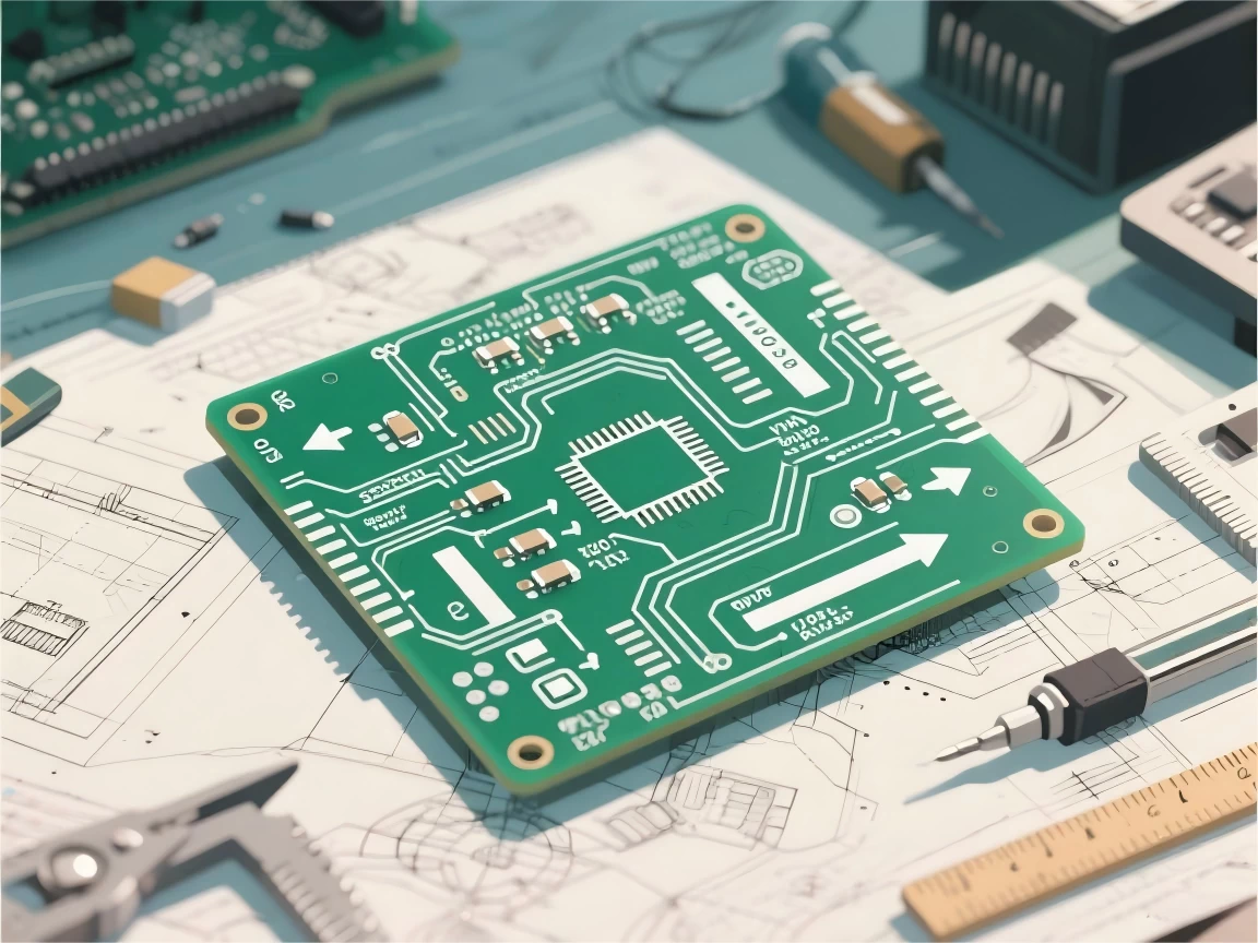
Internet of Things (IoT) is transforming sectors from consumer goods to healthcare and agriculture, making Printed Circuit Board (PCB) design for these devices increasingly vital. At the core of IoT’s revolutionary potential lies seamless wireless data exchange, a function fundamentally reliant on the PCB. This intricate communication between interconnected devices requires a strong, reliable foundation, which the PCB provides.
When it comes to PCB design and fabrication, IoT devices demand compact, power-efficient, and high-performance PCBs to fulfill their specialized roles and withstand diverse environmental conditions. The need for miniaturized devices and higher efficiency drives more design upgrades at various levels. This presents significant challenges, including limited physical space, stringent power budgets, and the critical need for robust wireless communication. Addressing these design complexities is paramount to ensuring IoT devices are not only functional but also durable and efficient in their interconnected environments.
In this article, we will look at some of the best PCB design optimization techniques to help manufacturers design more efficient IoT devices and systems. We will highlight the design challenges and their solutions, enabling designers with more space- and operationally friendly designs.
Suggested Reading: PCB Design Basics for New Designers – A Complete Guide
IoT Devices – A Quick Look
IoT devices are physical objects embedded with sensors, software, and network connectivity, enabling them to collect and exchange data over the internet without human intervention. They range from everyday smart home gadgets to complex industrial machinery.
A key advantage of IoT devices lies in their ability to:
- Enhance efficiency
- Automate processes
- Provide real-time data for informed decision-making
These devices are helpful across various industries like consumer, healthcare, and agriculture.

IoT Devices – A Quick Look
PCBs are a pivotal component of IoT systems, providing a viable platform to connect various parts of an IoT network, such as sensors, actuators, and microcontrollers. They house all IoT infrastructure and essential electronic components that facilitate:
- Rapid data processing.
- Storage and sharing.
More importantly, these boards enable both wired and wireless connections, allowing diverse electronic devices and systems to communicate seamlessly. This network of devices forms the foundation of IoT technology.
In the modern age, IoT circuit boards are ubiquitous, powering everything from smart home systems, consumer products, and healthcare devices to advanced applications in agriculture, automotive, and industrial equipment.
Why Efficient PCB Designs are Needed in IoT Sector
Designing Printed Circuit Boards (PCBs) for the vast and varied IoT ecosystem is complex, requiring compact, energy-efficient, and high-density layouts. These demands are not merely beneficial but essential for devices operating across diverse environments.
| Statistic | Figure | Source | Significance for IoT PCB Design |
|---|---|---|---|
| Projected IoT data generated by 2025 | 79.4 Zettabytes | Statista | Highlights the need for robust data processing and storage on PCBs. |
| IoT devices as % of all connected devices by 2025 | >50% | Statista | Underscores the pervasive demand for specialized IoT PCBs. |
| Percentage of IoT devices reliant on battery power | 85% | Business Insider | Emphasizes the critical importance of power-efficient PCB designs. |
PCB Design Optimization Techniques for IoT Devices
PCB design optimization is essential for signal integrity, flawless connectivity and transmission, IoT device usability, and cost compliance. In this regard, here are some useful PCB design optimziation techniques for IoT devices
Miniaturization and Form Factor Reduction
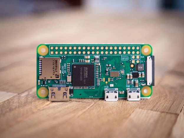
Miniaturization is a crucial optimization technique for PCBs in IoT devices. It is driven by the need for compact designs across their varied applications, from wearables to smart sensors. In this regard, multilayer PCBs are critical as they offer the necessary space to integrate diverse components, antennas, and routing within a minimal footprint.
Miniaturization offers several benefits, like:
- Reduced product size.
- Improved portability.
- Ability to integrate into smaller enclosures.
At the same time, the small form factor also introduces significant design complexities. Hence, designers must meticulously consider trace widths, via placements, and component sizes, demanding efficient space utilization without sacrificing functionality. This includes the potential use of micro-electromechanical systems (MEMS) components for even smaller board designs.
Power Management
Designing power-efficient PCBs for IoT devices is crucial and begins with selecting low-power components. Therefore, designers must opt for microcontrollers (MCUs) with effective sleep modes and low-voltage operation. Moreover, picking sensors that function efficiently in low-power states is a critical aspect of power management in IoT devices.
Energy-efficient wireless modules like Bluetooth Low Energy (BLE) or LoRa are therefore a popular choice in modern industrial IoT applications.
Beyond component selection, power-gating and voltage regulation play a vital role, for instance:
- Power gating transistors selectively cut power to idle circuit blocks, preventing unnecessary energy drain.
- Low-Dropout Regulators (LDOs) minimize power loss during voltage regulation.
Also, optimizing clocking and sleep modes is an important power management aspect. Clock gating disables clocks to unused components, ensuring MCUs and wireless modules enter deep sleep states when idle. It means that designers can significantly reduce overall power consumption, extending battery life and improving device longevity.
Multilayer PCB Designs
Multilayer PCB designs critical for IoT device optimization. The address space constraints in PCB design by incorporating multiple layers. Their key advantages are as follows:
- They segregate power and signal traces, preventing interference and maintains signal integrity, especially crucial in high-density circuits.
- Multilayer PCBs integrate ground planes, which act as shields against Electromagnetic Interference (EMI), enhancing performance.
- They allow more components to be fitted into a compact footprint without compromising functionality.
This approach not only facilitates high-density interconnects in a smaller form factor but also allows for better thermal management through dedicated ground planes and heat control features like thermal vias.
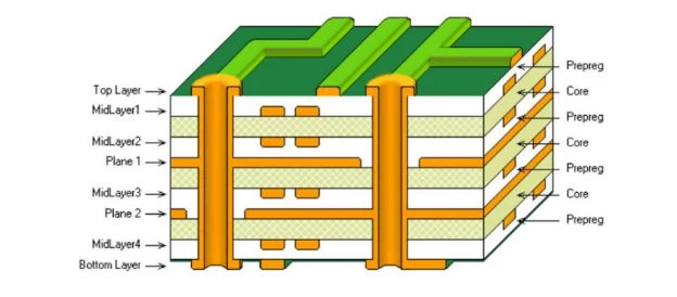
Moreover, advanced stack-ups enable the isolation of sensitive traces and seamless integration of mixed-signal and RF circuits on a single board, ensuring efficient IoT system operation. The number of layers chosen should always align with the board’s specific layout requirements to optimize both performance and cost.
Suggested Reading: Multi-layer PCB Stack-up Design Guideline.
Antenna Placement Optimization
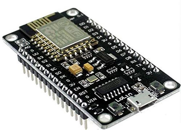
Wireless communication is the core of IoT. It is facilitated by strategic placement of antennas on the PCB, and therefore, is a critical optimization technique to guarantee robust performance. In most IoT boards like NodeMCU, Jetson Nano, and others, the orientation and precise positioning of antennas helps prevent signal interference and ensure maximum signal strength.
It involves employing techniques like
- Coplanar waveguides for efficient signal transmission,
- Incorporating impedance matching networks to maximize power transfer to the antenna,
- Using dedicated RF shields to isolate the antenna from other noisy components,
Eventually, it improves signal quality and minimizes losses.
Moreover, proper grounding and decoupling are essential to prevent noise and signal degradation that can compromise wireless connectivity. To refine this complex aspect of design, simulation tools are invaluable. These tools allow designers to accurately model the antenna’s performance, predict potential interference or signal mismatch issues, and analyze critical aspects such as signal reflection and antenna radiation patterns.
Catering EMI/EMC
Given their inherent wireless communication, IoT devices are particularly vulnerable to Electromagnetic Interference (EMI). To ensure optimal performance and compliance, designers must actively integrate EMI/EMC (Electromagnetic Compatibility) reduction strategies into the PCB layout.
EMI Shielding is crucial for managing both internal and external interference, especially when the board incorporates sensitive RF circuits or high-speed data transfer interfaces like USB, HDMI, and PCI.
Moreover, adhering to established EMC standards, such as those set by the Federal Communications Commission (FCC), ensures the device operates reliably without causing or succumbing to electromagnetic disturbances.
Minimized Trace Length and Width
Minimizing both trace width and length is a critical PCB optimization technique that directly impacts overall performance in compact designs. By making deliberate routing decisions, designers can significantly improve signal integrity, ensuring data is transmitted accurately and efficiently, while simultaneously reducing electromagnetic interference (EMI) within the dense layout.
This optimization is achieved through several methods:
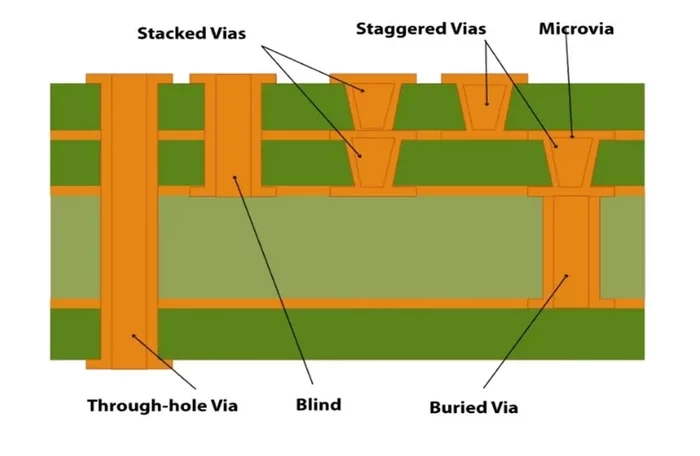
- Microvias - are increasingly utilized as they enable shorter trace lengths and better signal quality by allowing connections between layers in very small spaces.
- Controlled impedance routing is essential as it ensures that traces maintain a consistent impedance, signal reflections are minimized, particularly for high-speed transmission.
Further Reading: PCB Trace Width VS Current Value Calculator
Security and Privacy
Data security is one of the core components of modern IoT devices. Securing wireless communication against cyber attacks is key to epansion and growth of IoT networks across the globe. As more IoT devices are developed, the vulnerability to cyberattacks continues to grow.
Hence, to cater such threats, PCB optimization techniques must include:
- Encryption
- Secure boot options
- Hardware-based authentications
More importantly, these security measures must work flawlessly with the existing wireless connectivity security features to ensure secure data transmission across geographical spots.
Challenges in PCB Design for IoT Systems
| Design Challenge | Description | Impact on IoT Devices |
|---|---|---|
PCB Cost & Function | Balancing feature integration and performance requirements with strict cost constraints for mass production. | Directly affects profitability and market competitiveness by influencing material, layer count, and component choices. |
Thermal Management | Dissipating heat generated by densely packed components to prevent overheating and maintain reliability. | Critical for device longevity and consistent performance, especially in sealed enclosures or high-temperature environments. |
Wireless Performance | Ensuring optimal signal strength, minimal interference, and reliable connectivity across various protocols. | Directly impacts data transmission reliability, range, and overall device functionality in an interconnected ecosystem. |
PCB Material Choice | Selecting the appropriate substrate material based on electrical properties, thermal stability, cost, and durability requirements. | Dictates signal integrity (especially at high frequencies), thermal dissipation, mechanical robustness, and overall manufacturing cost. |
Conclusion
Optimizing PCB design is essential for the success of IoT devices. These techniques directly address challenges like miniaturization, power efficiency, and cost. Moreover, techniques such as employing multilayer PCBs for high-density layouts, meticulous trace management for signal integrity, strategic antenna placement for robust wireless performance, and comprehensive EMI/EMC mitigation are vital.
By carefully considering these optimization strategies and the inherent design challenges, engineers can create IoT devices that are not only compact and efficient but also reliable and performant in diverse environments.
FAQs
1. Why is PCB optimization so critical for IoT devices?
Optimized PCBs are essential for IoT devices to achieve compact size, low power consumption, high performance, and reliable wireless connectivity in diverse and often challenging environments.
2.How do multilayer PCBs benefit IoT designs?
Multilayer PCBs maximize space, allowing for high-density component integration and efficient routing while separating sensitive signals and providing better EMI shielding in a small footprint.
3.What techniques ensure optimal wireless performance on an IoT PCB?
Proper antenna design and placement, meticulous trace management (e.g., controlled impedance), effective grounding, and EMI/EMC mitigation strategies are key to robust wireless connectivity.
4.How is power efficiency achieved in IoT PCB design?
Power efficiency is optimized by selecting low-power components (MCUs, sensors, wireless modules), implementing power-gating, and utilizing deep sleep modes for idle circuits.
5.What are the main challenges in designing PCBs for IoT?
Key challenges include miniaturization, thermal management, ensuring robust wireless performance, managing costs while integrating complex functionality, and selecting appropriate PCB materials for the application.
References
- PCB Design for IoT Devices: Challenges and Solutions for Compact, Efficient Boards
- PCB Design for IoT Devices: Efficient & Compact Layouts
- 5 Tips to Optimize PCB Design for IoT Applications
- Multilayer PCBs and the Cutting-Edge of Circuit Board Repair
- IoT PCB Design Challenges and Best Practices
- EMI Shielding: Protecting Electronic Devices in a Noisy World