Skip to content
  • +86-755-8487 1176
  • [email protected]
logo
  • PCB Layout
    • PCB Design
  • Engineering
    • Mechanical Engineering
  • Services
    • PCB Manufacturing
    • PCB Assembly
    • PCB Reverse Engineering
    • 3D Printing
    • Components Procurement
    • Electronic Hardware Design
    • Software & Firmware Development
    • Electronics manufacturing services
  • About us
    • Why Us
    • How We Work
    • Career
    • Blog
  • Contact Us
  • FAQ
Advanced PCB silkscreen design showing component labels and logos.

Advanced Uses of PCB Silkscreen in PCB Design

November 28, 2025

Printed Circuit Board (PCB) silkscreen is an essential and multifaceted element in modern electronics design and manufacturing. It refers to the layer of non-conductive ink

Read More »
Visual flowchart for optimizing PCB design for production, outlining key DFM checks for panelization, trace spacing, annular rings, and solder mask slivers to maximize fabrication yield and minimize cost.

PCB Design Optimization for Compact and Connected IoT Devices

June 21, 2025

An-embedded-IoT-microcontroller-board Internet of Things (IoT) is transforming sectors from consumer goods to healthcare and agriculture, making Printed Circuit Board (PCB) design for these devices increasingly
Read More »
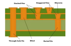
PCB-stackup-with-Copper-Filled-Microvias

Blind and Buried Vias – Advanced PCB Interconnect Technologies

May 17, 2025

The-illustration-of-high-density-PCB-holes-structures The industrial applications of printed circuit boards continue to increase across various sectors. The ever-growing need for smaller, faster, and more feature-rich electronic devices
Read More »
How-to-make-a-Cost-Effective-PCB-Fabrication

The Best Design for Manufacturing (DFM) Practices for Cost-Effective PCB Fabrication

April 28, 2025

The Best Design for Manufacturing (DFM) Practices for Cost-Effective PCB Fabrication Printed Circuit Boards (PCBs) are everywhere around us. Regardless of the industry types, they
Read More »
PCB-Power-and-Ground-Planes-Design-guidelines

The Importance of Power and Ground Planes in PCB Design

April 21, 2025

Ground and Power planes are large copper areas on the PCB that are engineered, designed, and placed to provide a stable return path for electrical
Read More »
PCB-Design-For-Manufacturing

PCB Design Basics for New Designers – A Complete Guide

April 14, 2025

Working with electronics is a journey, and in this journey, we all start with basic electronics with bread boards and perfboards and venture our way

Read More »
« Previous Page1 Page2 Next »
Tags
Chinese PCB Design Circuit Board Layout Component Placement Design for Assembly (DFA) Design for Excellence Design for Manufacturing Design for Manufacturing (DFM) DFM DFM Checklist Electronics Design Electronics Engineering Outsourcing Fast Prototyping First-pass Success Hardware Design Hardware Engineering Hardware Startup HDI PCB IP Protection Learn PCB Design PCB-Design PCB-Fabrication PCB-layout PCB Assembly PCB Best Practices PCB Design for Manufacturing PCB Design for SMT PCB Design Services PCB DFM PCB Manufacturing PCB Manufacturing China PCB Routing PCB Stackup PCB Tips PCB Tutorial Pick and Place Reflow Soldering Signal Integrity SMT Assembly SMT Manufacturing Solder Bridging Solder Joint Reliability Solder Paste Stencil Supply Chain Technical Illustrations Visual Guide

Address

201, Block S, Hengyu, Science&Technology Park, No.1 Ruiji Rd, Nanlian Community, Longgang District, Shenzhen, China.

Email

[email protected]

Phone

+86 755 8487 1176

Get In Touch With Us Today

Drag & Drop Files Here (dsn, pdf, xlsx, dxf, zip, rar up to 8M)
or
Browse Files
logo

At RockPCB, LLC. we strive to be your premier partner in technological design engineering, offering comprehensive solutions from circuit board design and layout to software and firmware development. Our mission is to provide applicable, intelligent solutions that propel our clients’ technologies forward.

Services

  • Reverse Engineering
  • PCB Reworking
  • PCB Assembly
  • Functional Test
  • Component Souring
  • PCB manufacturing
  • Reverse Engineering
  • PCB Reworking
  • PCB Assembly
  • Functional Test
  • Component Souring
  • PCB manufacturing

Quick Links

  • Home
  • Blog
  • Privacy Policy
  • Home
  • Blog
  • Privacy Policy

Contact Info

  • 201, Block S, Hengyu, Science&Technology Park, No.1 Ruiji Rd, Nanlian Community, Longgang District, Shenzhen, China.
  • +86 755 8487 1176
  • [email protected]
© 2025 RockPCB LLC. All Rights Reserved.