The Best Design for Manufacturing (DFM) Practices for Cost-Effective PCB Fabrication
Printed Circuit Boards (PCBs) are everywhere around us. Regardless of the industry types, they are pivotal in today’s manufacturing setup. So, it’s understandable how efficient and accurate PCB designs can leverage efficiency in the industrial sectors.
The design phase is the most pivotal in PCB manufacturing. More than two-thirds of PCB manufacturing issues occur due to flawed design practices. And the only way to prevent these issues is to ensure the best design for manufacturing (DFM) practices, ensuring cost-effective operations and enhanced production quality.
This guide will take you through some critical aspects of Design for Manufacturing (DFM) that can help design engineers optimize designs according to the PCB manufacturer’s requirements, ultimately cutting down the cost of PCB fabrication.
Recommended Reading: About Printed Circuit Board, What You Need to Know
What is Design For Manufacturing (DFM)?
PCB Design for Manufacturing (DFM) is a process that optimizes the PCB design according to the manufacturer’s requirements. It involves a series of steps to ensure the design is easy and efficient for manufacturing
For instance, when a manufacturer wishes to design a PCB for a device, DFM will aim to ensure that the electronic parts of the PCB fit well. Therefore, DFM involves the analysis of critical product aspects such as:
- Functionality
- Materials
- Tolerances
- Dimensions
These inspections are carried out by certified contractors who examine various product ideas to pick optimal materials, measurements, and processes. These measures ensure that manufacturers can yield benefits such as:
- Reduced overhead.
- Enhanced product quality.
- Identification of alternative manufacturing methods for short production runs.
- Facilitation of cost-effective solutions for unique measurements.
- Improvement of existing designs by identifying and eliminating wasteful steps in the manufacturing process
How DFM Practices Help in Cutting Costs
Design for Manufacturing (DFM) in PCB design is an approach to reduce costs. It does so by considering the board’s production during the layout phase. Implementing DFM early streamlines both the board fabrication and the component assembly processes.
Furthermore, DFM emphasizes using standard electronic components and their connection layouts (footprints). This standardization leads to lower costs when buying the parts and makes the assembly process simpler. By following DFM guidelines, potential problems that could occur during manufacturing can be spotted and fixed during the design stage.
This proactive approach minimizes the need for expensive redesigns, fixing errors, and production delays, ultimately improving the number of good boards produced and reducing wasted materials, resulting in better overall cost efficiency.
An Example of DFM
Suppose you design a PCB for an automated assembly line that will place the components on the PCB. Without a DFM, you may face one or more of the following problems:
- The machines can’t easily place tiny parts.
- The soldering process may create errors
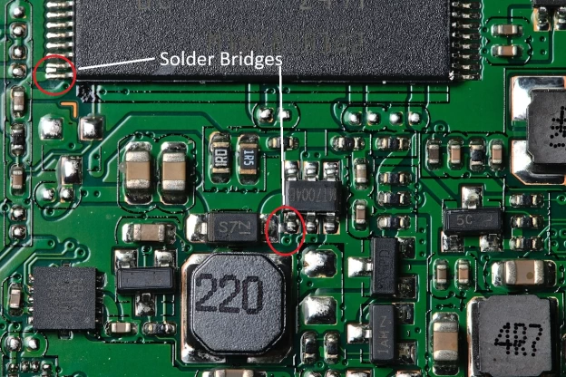
A DFM process would optimize the design, suggesting enough space between components to allow pick-and-place machines for accurate placement. This will eventually prevent solder bridges. A simple design change could speed up the production process with fewer defects.
But an equally important benefit of DFM is cost optimization. Here is how DFM reduces cost in our example:
Fewer Manufacturing Defects: Fewer defects mean less rework and fewer scrapped boards. It saves time, labor costs, and reduces material waste.
Faster Assembly: The assembly process speeds up when components are easier for pick-and-place machines to handle accurately. This reduces the overall manufacturing time, and reduces labor cost per board.
Higher Yields: A smoother manufacturing process with fewer defects and easier assembly leads to a higher yield, with more functional PCBs coming off the assembly line. This means more sellable products for the same initial investment, increasing profitability.
The Best Design For Manufacturing Practices
DFM encircles a broad area from dimensions to functionality. Hence, several design aspects can help you optimize your PCB design. Here are some of critical DFM practices to consider.
1. Reduce PCB Components
A DFM process would optimize the design, suggesting enough space between components to allow pick-and-place machines for accurate placement. This will eventually prevent solder bridges. A simple design change could speed up the production process with fewer defects.
A minimalistic PCB design is key to avoiding complications during the manufacturing phase. Fewer PCB components ensure easier fabrication and reduce board complexity. So, to reduce the PCB components, designers must thoroughly examine each part, analyzing which components can be replaced, combined, or completely removed from the PCB design.
Hence, using multifunctional components can help in reducing the component count. Likewise, using integrated circuits instead of individual components can be an alternative to achieving the same functionality. Here, it is important to consider that the overall functionality of the board is not compromised. So, considering thermal characteristics, voltage and current ratings becomes a critical aspect while reducing PCB component count.
Example of Component Reduction
Here are a few examples how designers can reduce PCB components.
- Using a resistor network (DIP or SIP package) instead of individual resistors for multiple input pins on a microcontroller. It also makes the placement algorithm simpler for pick and place machines.
- Replacing individual diodes for rectifier gates with dedicated rectifier ICs.
- Using microcontrollers with internal pull-up or pull/down resistors.
- Using a multiple LED driver IC instead of individual current-limiting resistors.
Cost Saving with Component Reduction
By using multi-functional or integrated components, the total component count on the PCB is reduced, which leads to:
- Lower Bill of Materials (BOM) cost.
- Faster assembly time (fewer parts to place).
- Simpler pick and place algorithms.
- Fewer solder joints, increasing reliability.
- Potentially smaller PCB size, further reducing material costs.
2. Strategic Component Placement
PCB components need to be placed strategically. It smoothens the assembly and manufacturing process. While it sounds intriguing to add components in a close vicinity, it’s not always practical considering the various characteristics of each component.
Poorly placed PCB components can be a costly step, eventually leading to flawed designs and increased manufacturing costs. Among the basic considerations for component spacing, the following aspects are most important:
- Component Assembly
- Board Testing
- Component Characteristics
The following table summarizes these critical spacing considerations:
| Component Assembly | Board Testing / Repair | Component Characteristic |
|---|---|---|
| - |
How Component Spacing Affects Cost
Simplified Testing: Strategically placed components with enough clearance facilitate easier access for test probes, enabling faster and more reliable automated testing. This lowers testing costs and ensures quality.
Lower Tooling Costs (Potentially): Designing for standard component footprints and avoiding extremely dense layouts might prevent the need for highly specialized and expensive assembly or soldering tools.
Optimized Material Usage: While seemingly counterintuitive, preventing assembly errors and rework through proper spacing minimizes the waste of expensive PCB materials and components.
3. Wire Routing Optimization
Wire routing suggests how much copper your PCB shall be consuming in terms of traces, vias, and pads. Ensuring a proper route makes signal transmission smoother and less prone to interference, ultimately improving board performance.
To optimize wire routing, it is critical to uphold the standard wiring practices. Additionally, the following considerations can improve PCB efficiency.
- Using 45-Degree or Rounded Corners: Routing traces with 45-degree angles or smooth curves eliminates acid traps, ensuring more consistent and reliable etching. This reduces the likelihood of trace defects and increases manufacturing yield, lowering the overall cost per board.
- Maintaining Consistent Trace Widths: Keeping consistent trace widths for signals with similar current-carrying requirements simplifies the manufacturing process and improves predictability. This can allow for looser manufacturing tolerances (reducing cost) without compromising functionality.
- Optimized Layer Usage: Intelligent routing minimizes the number of layer changes (via usage). Fewer vias mean fewer drilling and plating steps, directly reducing manufacturing costs and improving signal integrity.
4. Modular / Multipurpose Board Designs
A modular design refers to creating function-specific modules that can be reused in various PCB designs. It makes the PCB a combination of various smaller functional blocks that may appear in other products too.
Modular designs reduce the complexity that may occur, otherwise. It simplifies the design, making it easier to read and troubleshoot.
Example of a Modular Design
Think of a control system PCB for a robotic arm. Instead of one large, complex PCB containing everything, a modular design can break it down into:
- A power supply module: Responsible for voltage regulation and distribution.
- A motor control module: Containing the drivers and feedback circuitry for each motor.
- A sensor interface module: Handling the input from various sensors.
- A communication module: For interfacing with a central controller.
- A processing core module: Containing the microcontroller or processor.
Each of these modules can be designed and even fabricated separately. They would then connect via standardized interfaces (like connectors or specific pin headers) on a mainboard or directly to each other. More importantly, you can use these modules for other applications too.
How Modules Save Cost
Modular designs ensure consistency in terms of component selection. Therefore, designers can create a module and use the same component specifications, which means a possibly lowered price per component for the manufacturer. Reduced component diversity also means designers can order components in bulk which is also a critical factor in reducing fabrication cost.
Potential Mistakes to Avoid During DFM
Having seen the best DFM practices, it is also important to look at some of the common mistakes that must be avoided during DFM analysis.
- Insufficient Edge Clearance: Failing to maintain adequate space between copper features (traces, pads, planes) and the board edge can lead to shorts or damage during the depanelization (separating individual boards) process.
- Creating Acid Traps: Sharp, acute angles (less than 90 degrees) in trace routing can trap etching chemicals (acid) during the manufacturing process. This can result in over-etching at the corners, leading to narrowed or broken traces, which compromises the electrical integrity of the circuit.
- Absence of Solder Mask: Omitting solder mask from areas that shouldn’t be soldered can lead to unintended solder bridges between pads during component assembly. Solder mask acts as an insulator, preventing shorts and ensuring solder flows only to the intended connection points.
Complex Board Layout: Overly dense component placement, excessive layer counts without necessity, and convoluted trace routing increase manufacturing - complexity and cost. This can lead to lower yields, longer assembly times, and difficulties in testing and rework.
Suggested Reading: Top 10 DFM Issues that Affecting PCB Manufacturing.
Conclusion
Embracing Design for Manufacturing (DFM) principles throughout the PCB design process is a strategic requirement for cost-effective and high-quality electronic product realization. By proactively considering manufacturability – from optimal component placement and spacing to meticulous routing and avoiding common issues like insufficient edge clearance and acid traps – designers can significantly streamline production, improve yields, and minimize costly rework and delays. Ultimately, a commitment to DFM translates into tangible financial benefits, enabling the efficient creation of reliable and competitive electronic devices in today’s demanding market
FAQs
1. What does "DFM" stand for, and what's the main idea behind it for making circuit boards?
DFM stands for “Design for Manufacturing.” The main idea is to design a circuit board (PCB) in a way that makes it easy and cost-effective to actually build in a factory. It’s like planning how to build something simple so the machines can do it quickly and with fewer mistakes.
2. Why is it important to think about how a PCB will be made while we are designing it?
If we don’t think about manufacturing during the design, we might create a design that’s very difficult or expensive to build. For example, if parts are too close together, the machines might not be able to place them correctly, leading to errors and wasted materials. Thinking about manufacturing early helps us avoid these problems.
3. The article mentioned "component spacing." Why does leaving enough space between parts on a PCB matter for making it?
Leaving enough space between the electronic parts on a PCB makes it easier for the machines to pick them up and put them in the right place. It also helps prevent problems during soldering, where the melted metal can accidentally connect the wrong parts if they are too close together. More space usually means fewer mistakes and a smoother building process.
4. What's one simple mistake in PCB design that DFM tries to help us avoid, and why is it bad for manufacturing?
One simple mistake is making the wiring paths (traces) with very sharp corners. During manufacturing, chemicals are used to create these paths, and sharp corners can trap these chemicals. This can lead to the wires being thinner or even broken, making the circuit board not work. DFM suggests using smoother, rounded corners for the wiring.
5. How can following DFM rules help make circuit boards cheaper to produce?
By following DFM rules, we make the process of building the circuit boards easier and with fewer errors. Fewer errors mean less time spent fixing mistakes (rework) and fewer boards that have to be thrown away (waste). When the manufacturing process runs smoothly and efficiently, the overall cost to produce each circuit board goes down.
References
- Design for Manufacturing (DFM) Considerations for PCB Design
- PCB Design Guidelines for Manufacturing (DFM)
- PCB Design For Manufacturing (DFM) Guidelines | MCL
- PCB Design for Manufacturing (DFM) Guidelines and Checklists – NCAB
- PCB Design for Manufacturing (DFM): Best Practices and Optimization Strategies for 2024 – Camptech II Circuits Inc.
- PCB Design For Manufacturability With Allegro X | Cadence