In the dynamic world of PCB manufacturing, achieving first-pass success relies on more than just cutting-edge manufacturing equipment and a skilled team. At RockPCB, we’ve witnessed countless successful launches of advanced HDI circuit board designs, all of which can be directly attributed to early collaboration between PCB designers and manufacturers during the initial design phase.
Unfortunately, in the PCB industry, cooperation often begins only after problematic issues arise—such as field failures, assembly repercussions, or low manufacturing yields. This reactive approach is the wrong starting point for collaboration.
When problems emerge late in the design cycle or during production, the cost to fix them increases exponentially. Redesigns, delays, and rework introduce unnecessary complexity and expenses while compromising product reliability and time-to-market. To avoid these challenges, collaboration must begin early in the design cycle to proactively address potential issues.

Bridging the Knowledge Gap
PCB designers often focus on functionality, performance, and compliance with end-use requirements, while PCB manufacturers pay closer attention to manufacturability, process efficiency, and cost optimization. Therefore, proactive collaboration between designers and manufacturers ensures alignment of capabilities and specifications from the outset, effectively minimizing potential discrepancies between design intent and production results.

Prevent Expensive Redesigns
Redesigns can be one of the most costly and time-consuming obstacles in PCB manufacturing. Learning from our past production experiences, issues frequently arise such as improper pad and drill sizes, drilled copper violations, material incompatibilities, or unbalanced stack-up structures, mismatched impedance. When these problems are presented to a designer’s attention, the typical first response is to push forward as it is or implement only minor, quick modifications in hopes the manufacturing issues will resolve themselves. This firefighting strategy, often driven by budget constraints and NPI schedule pressures, severely limits opportunities for thorough DFM analysis to eliminate root causes of yield loss.
This habitual decision-making cycle has far-reaching consequences. Hurry redesigns may lead to:
- Product performance compromised
- Field reliability reduced
- Waste of time and loss of money
- Increased financial costs from remaking production
- Delayed schedule, and missed market opportunities, eroding a company’s competitive advantage
To break free from this cycle, we must shift our focus from simply ‘fixing problems’ to thoroughly preventing them altogether through early collaboration. This proactive mindset creates opportunities for Design for Manufacturability (DFM) from the outset, leveraging manufacturers’ expertise to identify potential risks before they become a roadblock.
Involve Manufacturers from the Initial Design Phase
By working together from the initial design phase, designers and fabricators can optimize key parameters such as layer count, via configurations, material selections, controlled impedance, and tolerances. These optimizations lead to higher yields, particularly for first-pass production, which saves time and reduces overall manufacturing costs, sometimes. It would be even more optimal to involve SMT assembly manufacturers from the initial design phase.
Importance of Enhanced DFM
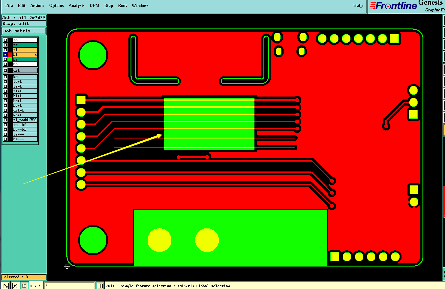
PCB manufacturers’ advanced CAM (Computer-Aided Manufacturing) DFM tools (such as Genesis2000) provide value inputs on design rules and constraints to the processes upon factory’s actual manufacturing capability: such as minimum trace width, spacing, and drill hole dimensions. These software tools have evolved significantly, offering powerful simulations that go beyond basic checks.
For example, today’s advanced DFM software tools can now simulate microvia reliability and predict potential bow-and-twist issues during PCB fabrication, allowing PCB designers to identify problematic designs before the layout begins.
Some key advantages of relying on advanced CAM DFM tools include:
- By simulating bow-and-twist issues during the design phase to prevent product failures and minimize material waste.
- Verifying and ensuring microvia reliability through simulation, reducing the risk of field failures.
- Enhancing long-term product reliability and durability.
- Streamlining the development process by eliminating back-and-forth design iterations.
- Speeping time-to-market and freeing up engineering resources for new product development.
- Reduces engineering evaluation cycle time at manufacturing facilities.
The cost benefits extend far beyond direct manufacturing expenses. Reliable first-pass yield minimizes material waste, avoids production delays, and prevents cascade effects of redesigns on other projects. This proactive approach ensures designs are optimized for manufacturability, ultimately delivering superior products faster and at lower total cost.
Collaboration in Action: Real-world Case
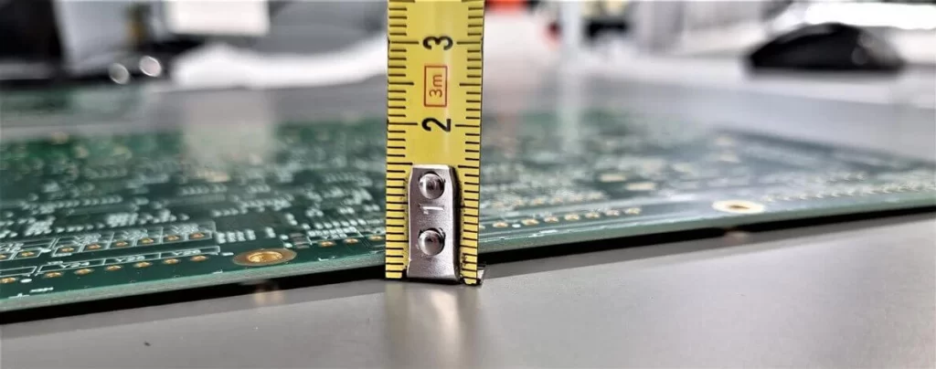
One of the most compelling examples of the value of early collaboration involved a client designing a 4L rigid PCB with unsymmetrical stack-up structure but required a constrained bow and twist value that not exceed 0.1%. The initial design of unsymmetrical stack up already addressed a significant manufacturing challenge and determined that the finished PCB would have warpage defects. The board’s original design resulted in a painful 25% final yield and less-than-desirable field reliability—a costly outcome for both the customer and the PCB fabricator.
Recognizing this issue, the PCB designer collaborated with the manufacturer to redesign the board through eliminating the root causes contributing to warpage. The redesign addressed the following critical problems:
- Stackup optimization
- Material compatibility
- Symmetrical copper distribution
The results of improving were remarkable. The revised revision achieved a 92% yield rate., a substantial improvement in manufacturability and reliability. This case highlights how proactive collaboration can transform a struggling design into a high-yield, reliable product, avoiding unnecessary costs and delays.

How to Establish Effective Collaboration
Effective collaboration between PCB designers and circuit board fabricators is essential for ensuring the success of a PCB project. Below are four proven strategies for building a strong partnership:
- Engage early – Designers should reach out to their fabricators during the initial phases of a project, particularly when designing the stack-up and selecting circuit board materials.
- Counting on expertise – Take advantage of the fabricator’s DFM and field engineering support services to validate designs and resolve potential issues up front.
- Effective Communicating – Share complete and accurate data packages, including clear design intent, specifications, and end-use application, to enable fabricators to have a thorough understanding to the purpose of the design and provide meaningful feedback.
- Build long-term relationships – Establishing a mutual partnership with a PCB fabricator creates a robust foundation for smoother collaboration on future projects, leading to continuous improvements in both PCB design and circuit board manufacturing processes.
Conclusion
Early-stage collaboration between PCB designers and circuit board manufacturers is no longer optional—it’s essential. The rewards of this approach are clear including:
- Reducing redesigns and avoiding production delays saves time and money.
- Reliable designs that succeed on the first pass will enhance product confidence.
- Accelerating Time-to-Market delivers competitive edge.
- Improved customer satisfaction and commercial reputation
Early stage collaboration enables circuit board manufacturers and PCB designers to consistently focus on the ultimate prize—being first to market with a dependable, cutting-edge product that sets them apart in the industry. Start planning now to ensure your next project is a success from the first pass.


