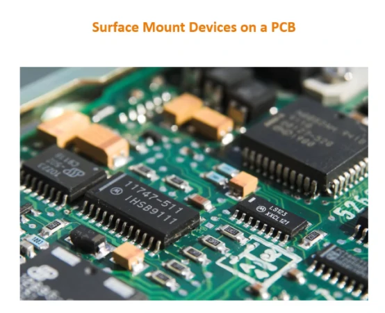
SMD stands for Surface Mount Device. It refers to an electronic component designed to mount directly onto the surface of a printed circuit board. Today, SMD technology powers smartphones, IoT devices, automotive electronics, medical devices, industrial controllers, LED products, and communication equipment.
Compared with traditional through-hole components, SMD parts use less board space, support faster automated assembly, and allow higher circuit density. At Fast PCB Layout, SMD technology is used every day in PCB fabrication, SMT assembly, component sourcing, and complete PCBA production.
Table of Contents
- What Does SMD Mean?
- SMD vs SMT
- Common Types of SMD Components
- Common SMD Packages and Sizes
- How SMT Assembly Works
- Advantages and Disadvantages of SMD Components
- Why Modern Electronics Use SMD Technology
- Design Considerations for SMD PCB Layouts
- Common SMD Assembly Defects and Quality Control
- SMD vs Through-Hole Components
- Applications of SMD Technology
- How Fast PCB Layout Supports SMD Projects
- Conclusion
- FAQs
What Does SMD Mean?
The SMD meaning in electronics is Surface Mount Device. An SMD is an electronic component that sits directly on copper pads on a PCB surface instead of passing through drilled holes. This structure allows engineers to design smaller, lighter, and more compact circuit boards.
Before SMD technology became common, most electronic assemblies used through-hole components. Those parts required long leads, drilled holes, and more manual work. As electronic products became smaller and more complex, manufacturers needed a faster and denser assembly method. SMD technology solved that problem.
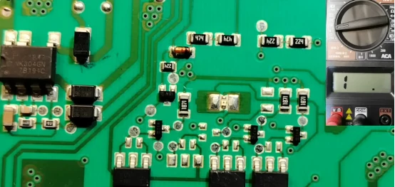
Today, almost every modern circuit board contains SMD components. Common examples include chip resistors, ceramic capacitors, inductors, diodes, transistors, microcontrollers, memory devices, sensors, and wireless modules.
SMD vs SMT
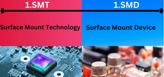
Many people use SMD and SMT interchangeably, but the two terms are different. SMD refers to the component itself. SMT refers to Surface Mount Technology, which is the process used to place and solder that component onto the PCB.
| Term | Full Name | Meaning |
|---|---|---|
| SMD | Surface Mount Device | The electronic component |
| SMT | Surface Mount Technology | The assembly process |
| PCBA | Printed Circuit Board Assembly | The finished assembled board |
For example, a 0603 resistor is an SMD component. The process that prints solder paste, places the resistor, heats the board, and forms the solder joint is SMT. If your project needs assembled boards instead of bare PCBs, PCB Assembly Services can help convert your design files and BOM into finished PCBAs.
5 Common Types of SMD Components
Most electronic components are now available in surface-mount versions. Engineers select them based on electrical function, package size, power rating, voltage rating, tolerance, temperature range, and assembly requirements.
SMD Resistors
SMD resistors limit current, divide voltage, set bias points, and control signal levels. They are among the most common components on modern PCBs because almost every circuit needs resistance control.
SMD Capacitors
SMD capacitors store electrical energy and stabilize voltage. Engineers use them for decoupling, filtering, timing, coupling, and noise reduction. In high-speed circuits, capacitor placement can strongly affect power stability.
SMD Inductors
SMD inductors store energy in magnetic fields. They are common in switching power supplies, RF circuits, filters, and DC-DC converters. Engineers must consider inductance, current rating, DC resistance, and thermal rise.
SMD Diodes and Transistors
SMD diodes control current direction, clamp voltage spikes, and protect circuits. SMD transistors switch or amplify signals in digital and analog systems. These components appear in power control, LED drivers, motor circuits, and protection networks.
SMD Integrated Circuits
SMD integrated circuits provide complex functions in compact packages. Examples include microcontrollers, processors, memory chips, power management ICs, sensors, and wireless communication chips.
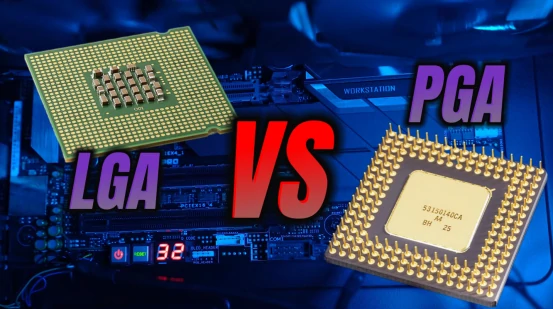
Common SMD Packages and Sizes
SMD package selection affects PCB density, assembly difficulty, thermal performance, inspection method, and rework capability. A smaller package can save space, but it may also require tighter process control.
Common IC Packages
| Package | Typical Use |
|---|---|
| SOIC | General-purpose ICs and analog circuits |
| TSSOP | Compact controllers and interface chips |
| QFP | Microcontrollers and control ICs |
| QFN | High-density and high-performance electronics |
| BGA | Processors, FPGAs, and memory devices |
| LGA | High-pin-count modules and processors |
Common Passive Component Sizes
| Package Size | Typical Use | Assembly Difficulty |
|---|---|---|
| 0201 | Wearables and compact modules | High |
| 0402 | Smartphones and IoT devices | Medium to High |
| 0603 | Industrial electronics | Low to Medium |
| 0805 | General electronics and prototypes | Low |
| 1206 | Power circuits | Very Low |
Many industrial and commercial products use 0603 and 0805 components because they balance space saving, assembly yield, inspection, and rework convenience. Very small packages such as 0201 help compact devices, but they require more precise placement and stronger process control.
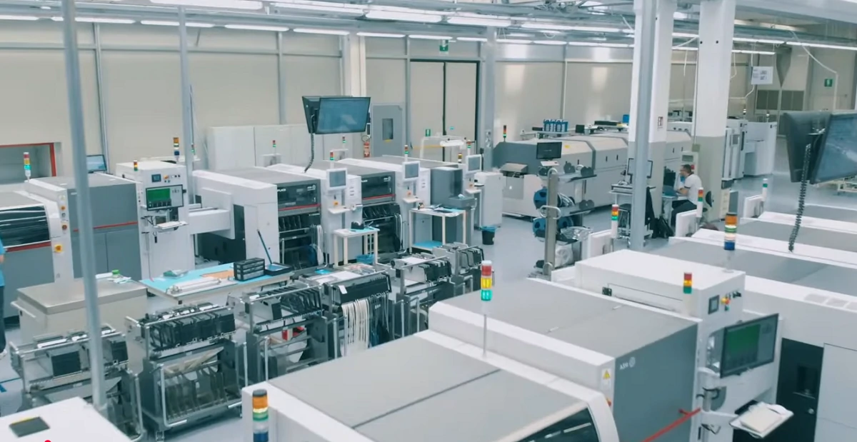
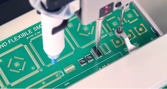
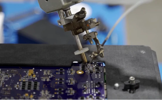
How SMT Assembly Works
SMT assembly is a controlled manufacturing process. Each step affects solder joint quality, production yield, and long-term reliability. A stable process depends on stencil design, solder paste control, placement accuracy, reflow profiling, inspection, and testing.
Solder Paste Printing
The process starts with solder paste printing. A stencil applies solder paste onto PCB pads. Correct paste volume is critical. Too much paste can cause solder bridging, while too little paste can create weak joints or open circuits.
Pick-and-Place Assembly
Automated pick-and-place machines position SMD components onto the solder paste. Cameras, feeders, nozzles, and placement software work together to place thousands of components per hour with high accuracy.
Reflow Soldering
The assembled board passes through a reflow oven. Controlled heating melts the solder paste and forms permanent electrical and mechanical connections. A poor temperature profile can cause tombstoning, voiding, cold joints, or component damage.
Inspection and Testing
After reflow, inspection systems check component placement and solder quality. AOI checks visible defects, while X-ray inspection checks hidden joints under BGA and LGA packages. For complete production support, Turnkey PCB Assembly can combine sourcing, fabrication, assembly, inspection, and testing in one workflow.
Advantages and Disadvantages of SMD Components
SMD technology became popular because it gives manufacturers clear benefits in size, speed, cost, and performance. However, it also creates new challenges in inspection, rework, process control, and thermal design.
| Advantages | Disadvantages |
|---|---|
| Smaller PCB size | More difficult rework |
| Higher component density | Requires SMT equipment |
| Faster automated assembly | Small parts are harder to handle |
| Lower cost at volume | Inspection can be more complex |
| Better high-frequency performance | BGA and QFN packages may need X-ray inspection |
For most modern products, the advantages are stronger than the disadvantages. SMD components allow more functions in a smaller space and support repeatable automated production. Still, engineers must consider repairability, assembly capability, heat dissipation, and inspection methods before final package selection.
Why Modern Electronics Use SMD Technology
Modern electronic products need smaller dimensions, higher performance, and lower production costs. SMD technology supports all three goals. It allows engineers to place more components in less space and often mount parts on both sides of the PCB.
SMD components also improve electrical performance. Their shorter connection paths reduce parasitic inductance and capacitance. This benefit is important in high-speed digital circuits, RF products, communication modules, and compact power designs.
Automated SMT production improves consistency and scalability. Instead of relying heavily on manual insertion, manufacturers can use controlled machines to place components with repeatable accuracy. This reduces variation and improves production efficiency.
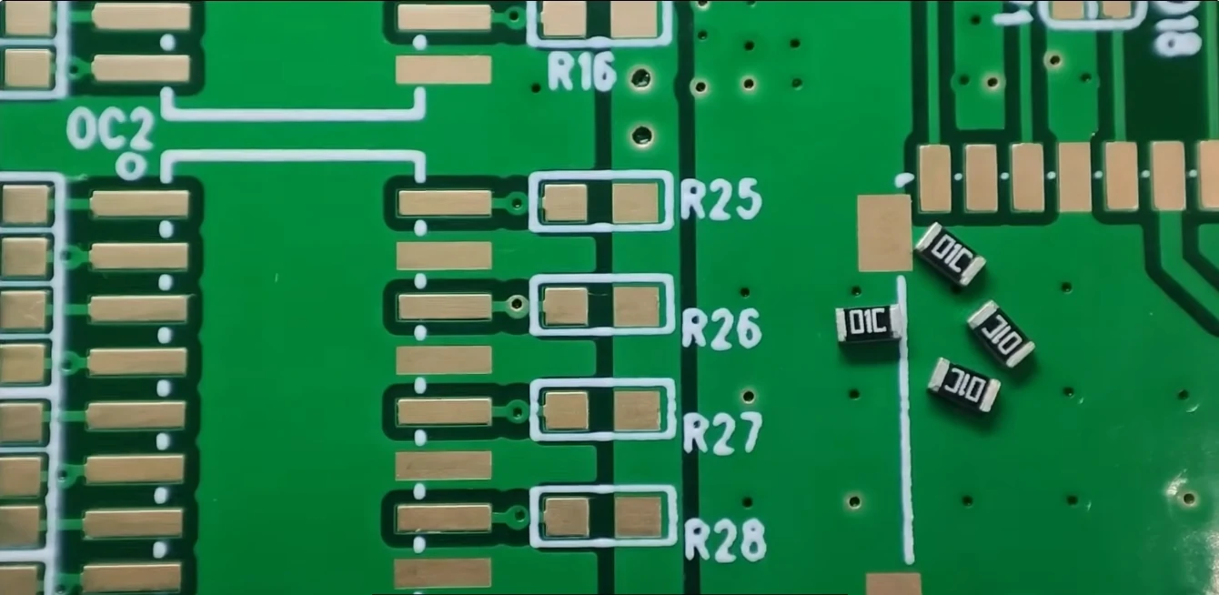
Design Considerations for SMD PCB Layouts
Successful SMT assembly begins with good PCB layout. A poor footprint or crowded layout can create defects even when the production line is well controlled. Engineers should review pad design, spacing, thermal paths, polarity marks, and manufacturability before release.
Pad Design
Pad geometry directly affects solder joint quality. Pads that are too large can pull components out of position. Pads that are too small can create weak joints. Designers should follow datasheet recommendations and manufacturing design rules.
Component Spacing
Adequate spacing helps prevent solder bridging and improves inspection access. Dense layouts may reduce PCB size, but they also increase assembly difficulty. Engineers should balance compact design with stable manufacturing.
Thermal Management
Power devices, LEDs, regulators, and processors generate heat. Designers often use copper pours, thermal vias, exposed pads, and wider traces to reduce temperature rise and improve reliability.
DFM Review
Design for Manufacturing review helps detect problems before production. DFM can check footprints, pad sizes, stencil openings, panelization, via placement, and component spacing. Our PCB Fabrication Services support manufacturability review before assembly.
Common SMD Assembly Defects and Quality Control
SMD assembly defects usually come from solder paste problems, placement errors, reflow profile issues, incorrect footprints, or component handling problems. Understanding these defects helps engineers improve production yield and long-term reliability.
| Defect | Common Cause | Impact |
|---|---|---|
| Tombstoning | Uneven solder wetting or thermal imbalance | Open circuit |
| Solder Bridging | Excess solder paste or tight pad spacing | Short circuit |
| Voiding | Poor reflow profile or trapped gas | Reduced reliability |
| Missing Components | Feeder, nozzle, or placement error | Functional failure |
| Misalignment | Placement offset or poor pad design | Weak joints or shorts |
Quality control usually includes SPI, AOI, X-ray inspection, and functional testing. SPI checks solder paste before placement. AOI checks visible components and solder joints after reflow. X-ray inspection checks hidden solder joints under BGA, LGA, and some QFN packages. Functional testing confirms that the final PCBA works under real operating conditions.
SMD vs Through-Hole Components
SMD and through-hole technologies both remain useful. SMD is better for compact layouts and automated production. Through-hole is better for parts that need stronger mechanical support.
| Factor | SMD | Through-Hole |
|---|---|---|
| Board Space | Smaller | Larger |
| Assembly Speed | Faster | Slower |
| Production Cost | Lower at volume | Higher |
| Mechanical Strength | Moderate | Higher |
| Best Use | Compact electronics | Connectors and heavy components |
Many products use both methods. Designers often use SMD components for most resistors, capacitors, ICs, sensors, and control circuits. They may use through-hole parts for connectors, transformers, relays, terminals, and large components exposed to mechanical stress.
Applications of SMD Technology
SMD technology supports nearly every electronics industry. Consumer electronics use SMD components to make phones, laptops, tablets, wearables, cameras, and gaming devices smaller and lighter.
Automotive electronics use SMD parts in engine control units, battery management systems, sensors, radar modules, LED lighting modules, and infotainment systems. Industrial automation systems use SMD technology in PLCs, motor drives, sensors, and communication controllers.
Medical devices use compact SMD assemblies in monitoring equipment, diagnostic instruments, and portable electronics. Telecommunications products use SMD packages in routers, RF modules, base station equipment, and networking devices. Robotics, aerospace systems, smart home devices, LED lighting, and energy storage systems also depend heavily on SMD technology.
How Fast PCB Layout Supports SMD Projects
Weller PCB provides PCB fabrication, SMT assembly, component sourcing, prototype manufacturing, and volume production support. Our engineering team reviews PCB layouts, BOM files, package selections, placement requirements, and manufacturability concerns before production begins.
This review helps reduce assembly risk and improve product quality. It also helps identify footprint issues, unavailable components, difficult package choices, inspection requirements, and potential DFM problems before they affect production.
If you are developing a new product or preparing for mass production, you can request Instant Quotes for PCBA Solutions. Clear Gerber files, BOM data, pick-and-place files, and assembly drawings help engineers review your project faster and more accurately.
Conclusion
SMD stands for Surface Mount Device. It is the component technology behind most modern electronic products. Compared with through-hole components, SMD parts support smaller PCB layouts, faster automated assembly, lower production costs, and higher circuit density.
However, successful SMD manufacturing requires more than small components. Engineers must consider package type, PCB footprint, solder paste design, reflow profile, inspection method, thermal behavior, and DFM requirements. When these details are controlled well, SMD technology improves both product performance and manufacturing reliability.
FAQs
What does SMD stand for?
SMD stands for Surface Mount Device. It describes an electronic component designed to mount directly onto PCB surface pads.
What is the difference between SMD and SMT?
SMD is the component itself. SMT is the assembly process used to place and solder that component onto the PCB.
Is SMD better than through-hole technology?
SMD is usually better for compact products, high-density layouts, and automated production. Through-hole is still useful for connectors, terminals, and mechanically stressed components.
What is the most common SMD package size?
0603 and 0805 are common in many industrial and commercial products because they balance PCB density, assembly reliability, inspection, and rework convenience.
Can SMD components be soldered by hand?
Yes. Larger SMD parts such as 0805 resistors, SOIC chips, and some SOT packages can be soldered by hand. Very small packages and BGA packages usually require professional SMT equipment.