SMT stands for Surface Mount Technology. It is a PCB assembly method that places electronic components directly on the surface of a printed circuit board. If you work with electronics, you will see SMT in almost every modern device.
In this guide, we explain what is SMT, how the SMT process works, why engineers use it, and how you can choose the right SMT assembly partner for prototypes or mass production.
Table of Contents
- What Is SMT?
- SMT vs SMD vs PCBA
- How the SMT Process Works
- Common SMT Components and Package Types
- Advantages and Limitations of SMT
- SMT vs Through-Hole Technology
- SMT Design, Quality, and Defects
- SMT Cost, Applications, and Assembly Partner Selection
- Conclusion
- FAQs
What Is SMT?
SMT means Surface Mount Technology. This technology mounts electronic parts on the surface of a PCB instead of inserting long leads through drilled holes. The result is a smaller, faster, and more automated assembly process.
Surface mount technology replaced much of traditional through-hole assembly because electronic products became more compact. Smartphones, IoT sensors, LED drivers, medical devices, robotics controllers, automotive modules, and telecom equipment all depend on PCB SMT assembly.
The main value of SMT is simple. It allows engineers to place more components in less space. It also helps manufacturers build boards faster and with higher repeatability. Compared with older methods, SMT technology gives product teams more design freedom and better production efficiency.
At Fast PBC Layout , we support electronics teams with PCB fabrication, SMT assembly, and turnkey PCBA solutions for prototypes and production projects.
SMT vs SMD vs PCBA
Many buyers ask about SMT meaning in electronics, but they often confuse SMT with SMD and PCBA. These terms connect to the same manufacturing chain, but they describe different things.
| Term | Full Meaning | What It Means |
|---|---|---|
| SMT | Surface Mount Technology | The assembly process |
| SMD | Surface Mount Device | The component mounted by SMT |
| PCB | Printed Circuit Board | The bare circuit board |
| PCBA | Printed Circuit Board Assembly | The finished assembled board |
SMT is the method. SMD components are the parts. The PCB is the platform. PCBA is the completed product. For example, an SMT production line places SMD electro components on an SMD PCB board and creates a functional PCBA.
How the SMT Process Works
The SMT process uses machines, solder paste, heat, inspection, and testing. Each step affects SMT quality. A weak step can create defects, rework, or field failures.
1. PCB Preparation
The process starts with a bare PCB. The manufacturer checks board dimensions, solder mask quality, surface finish, and panel design. Common surface finishes include ENIG, HASL, and OSP. A better surface finish improves solderability and reliability.
Good PCB fabrication services help reduce soldering problems before assembly starts.
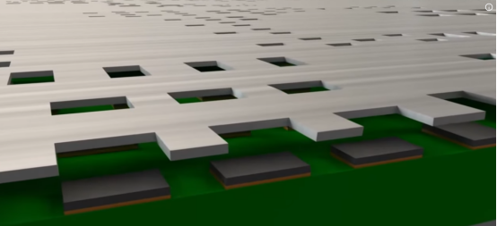
2. Solder Paste Printing
The SMT line applies solder paste to PCB pads through a stainless-steel stencil. Solder paste contains solder particles and flux. The stencil controls solder volume. More solder can cause bridging. Less solder can cause weak joints.
3. Solder Paste Inspection
SPI checks paste height, volume, area, and alignment. This step catches problems early. It is faster to fix paste defects before components enter the board.
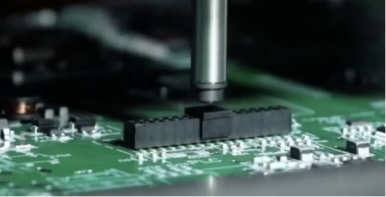
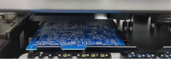
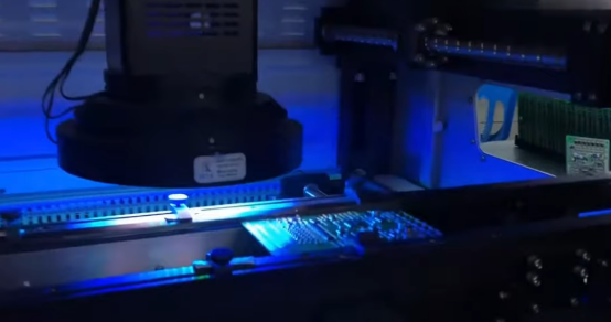
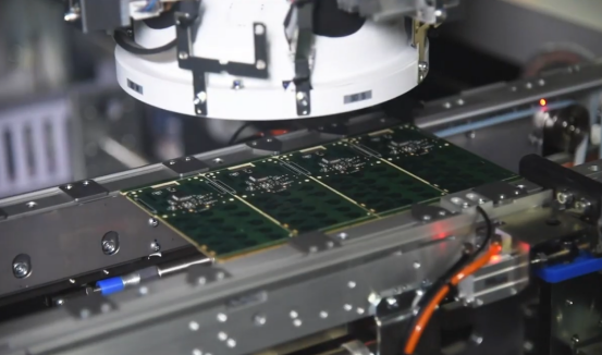
4. Pick-and-Place Assembly
Pick-and-place machines place SMT components on the solder paste. These machines use reels, trays, tubes, feeders, and camera systems. They place resistors, capacitors, ICs, QFNs, BGAs, and connectors with high speed and high accuracy.
5. Reflow Soldering
The PCB enters a reflow oven. The oven heats the board through preheat, soak, reflow, and cooling zones. The solder melts and forms joints. Then the solder cools and becomes solid. Lead-free solder often needs a higher peak temperature than tin-lead solder.
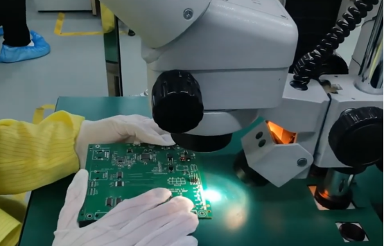
6. Inspection and Testing
AOI checks visible solder joints and placement errors. X-ray inspection checks hidden joints under BGA and QFN packages. ICT and functional testing check electrical performance. Strong inspection creates higher yield and more reliable products.
| SMT Step | Main Purpose | Common Risk |
|---|---|---|
| Solder Paste Printing | Apply solder paste | Too much or too little paste |
| Pick-and-Place | Place components | Misalignment or wrong polarity |
| Reflow Soldering | Create solder joints | Voids, bridges, cold joints |
| AOI/X-Ray | Inspect assembly quality | Hidden defects if inspection is weak |
Common SMT Components and Package Types
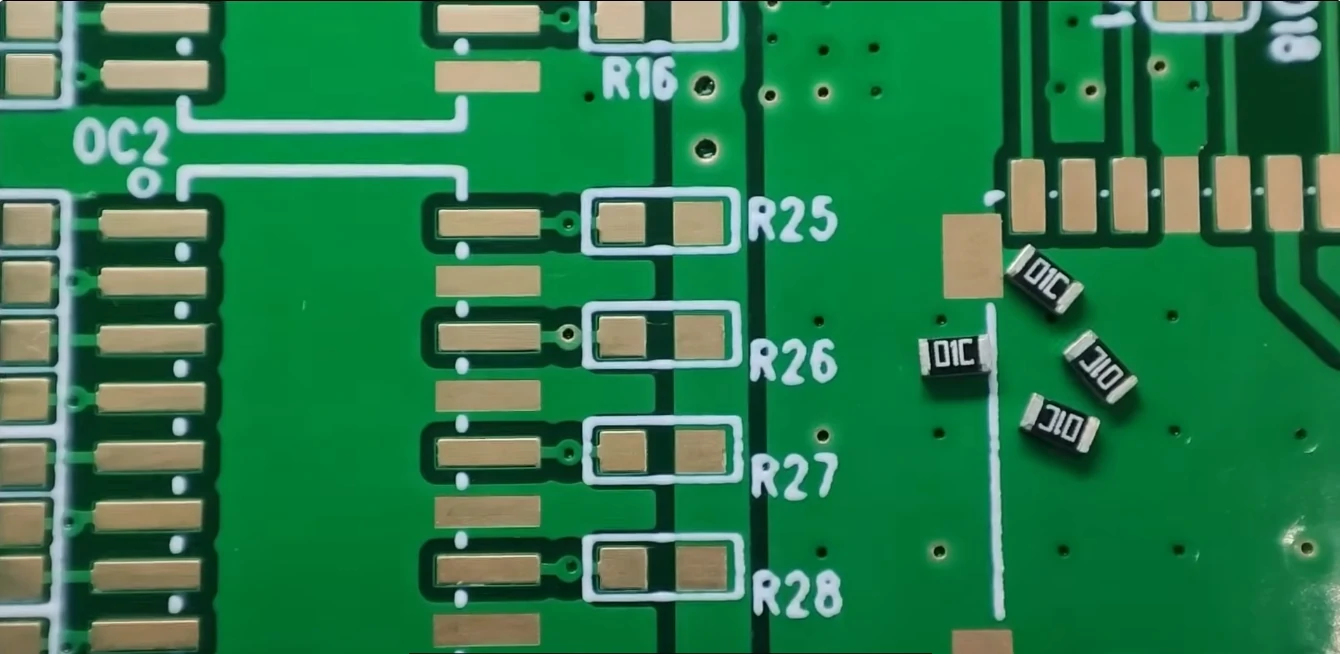
SMT electronics manufacturing uses many component types. Passive components include resistors, capacitors, and inductors. Active components include microcontrollers, processors, memory chips, power ICs, and sensors.
Small SMT components allow engineers to design more compact products. Common passive package sizes include 0805, 0603, 0402, 0201, and 01005. Smaller parts save space, but they require tighter process control.
Advanced SMT packages include SOP, SOIC, SOT, QFP, QFN, BGA, CSP, and PoP. BGA packages work well for high-pin-count devices. QFN packages offer better thermal performance than many leaded packages. PoP saves more board space than separate memory and processor packages.
Moisture-sensitive devices need careful handling. Some ICs require dry storage, baking, and ESD protection. Better material control improves solder joint reliability.
Advantages and Limitations of SMT
SMT gives engineers and manufacturers several strong advantages. It supports smaller designs, higher component density, faster production, and better automation.
Advantages of SMT
SMT components have shorter leads than through-hole parts. Shorter leads reduce parasitic inductance and improve high-frequency performance. This benefit matters more in RF circuits, high-speed digital boards, telecom modules, and compact IoT devices.
SMT also lowers assembly cost in many projects. Automated machines place components faster than manual labor. Smaller components also allow smaller PCB sizes. A smaller PCB can reduce material cost.
Limitations of SMT
SMT is not perfect. Tiny components are harder to repair. BGA solder joints are hidden under the package. Heavy connectors and high-current terminals may need through-hole support. High-density boards also need better thermal design.
| Factor | SMT Advantage | SMT Challenge |
|---|---|---|
| Board Size | Smaller and denser | Layout needs tighter control |
| Production Speed | Faster automation | Requires machine setup |
| Signal Performance | Better for high-speed circuits | Needs good PCB layout |
| Repair | Possible with tools | Harder than large THT parts |
SMT vs Through-Hole Technology
SMT and through-hole technology serve different needs. SMT places parts on the PCB surface. Through-hole technology inserts component leads through drilled holes and solders them on the other side.
SMT is faster and more compact. Through-hole is stronger for mechanical stress. SMT works better for most modern electronic circuits. Through-hole works better for large transformers, high-power components, connectors, and parts that face repeated plugging or vibration.
Many real products use mixed technology assembly. The board may use SMT for chips, resistors, and capacitors. It may use through-hole for connectors, relays, terminals, and mechanical parts. This hybrid method gives the board both compact performance and stronger mechanical support.
SMT Design, Quality, and Defects
Good SMT assembly starts with good PCB design. Engineers should use correct land patterns, clean polarity marks, proper component spacing, and useful fiducial marks. They should also review thermal pads, BGA escape routing, panelization, and test points.
A complete SMT quote usually needs Gerber files, BOM, centroid file, pick-and-place file, assembly drawing, and testing requirements. Clear files reduce engineering questions and shorten lead time. Professional PCB layout design services can also help teams prevent assembly issues during the design stage.
Common SMT Defects
SMT defects usually come from design, solder paste, placement, or reflow problems. Tombstoning happens when one side of a small chip lifts during reflow. Solder bridging happens when excess solder connects adjacent pads. Voiding often appears under thermal pads or BGA balls.
Other defects include insufficient solder, cold joints, solder balls, component shift, and head-in-pillow defects. Better stencil design, better reflow profiling, stronger AOI, and X-ray inspection can reduce these risks.
SMT Quality Standards
Professional SMT quality often follows IPC-A-610 and IPC J-STD-001. IPC Class 2 suits many commercial products. IPC Class 3 fits more demanding products, such as medical, aerospace, automotive, and mission-critical electronics.
SMT Cost, Applications, and Assembly Partner Selection
SMT cost depends on PCB complexity, component count, package type, inspection level, testing needs, and production quantity. A board with many BGAs usually costs more than a simple LED controller. Double-sided SMT assembly costs more than single-sided assembly because it needs extra process control.
Prototype SMT also differs from mass production SMT. Prototype builds need flexibility and engineering feedback. Mass production needs stable yield, repeatable quality, and controlled cost. Pilot production connects both stages.
SMT supports many industries. Consumer electronics use SMT for compact products. Automotive electronics use SMT for control modules and EV systems. Medical devices use SMT for patient monitors and diagnostic equipment. Industrial automation uses SMT for PLCs, sensors, and control boards. LED lighting, robotics, telecom, aerospace, and IoT products also depend on SMT.
When you choose an SMT assembly partner, you should check capability, quality systems, inspection equipment, sourcing support, and engineering experience. Ask about minimum component size, BGA capability, AOI, X-ray inspection, DFM review, component sourcing, and functional testing.
As a Fast PCB Board Manufacturer, we help engineering teams move from design to production with PCB fabrication, component sourcing, SMT assembly, and testing. For turnkey support, you can also review our PCB assembly services.
If you need pricing for prototypes, low-volume builds, or production PCBAs, you can request instant quotes for PCBA solutions.
Conclusion
SMT is the core assembly technology behind modern electronics. It helps engineers build smaller, faster, and more reliable products. It also helps manufacturers increase production speed and reduce cost through automation.
When you ask “what is SMT,” the simple answer is this: SMT is the process of mounting electronic components directly onto a PCB surface. The deeper answer is more important. SMT affects product size, signal performance, cost, reliability, inspection, and manufacturing scalability.
You should review SMT early in your design process. You should check footprints, solder paste needs, component spacing, inspection access, thermal paths, and testing plans. A strong SMT assembly partner can help you avoid expensive redesigns and production delays.
For engineering teams, OEM brands, startups, and sourcing managers, SMT is not just a manufacturing step. It is a key part of product success.
Frequently Asked Questions
What is the smallest SMT component size available today?
Most commercial SMT assembly lines can place 0201 components, while advanced SMT manufacturers can handle 01005 packages. Smaller components allow higher circuit density and more compact products, but they require more precise placement equipment, tighter process control, and better PCB layout design.
Can SMT and through-hole components be used on the same PCB?
Yes. Many electronic products use mixed-technology assembly. SMT components provide higher density and faster manufacturing, while through-hole components offer stronger mechanical support for connectors, transformers, relays, and high-current terminals. Combining both technologies often provides the best balance between performance and durability.
What files are required for SMT assembly?
Most SMT assembly providers require Gerber files, a Bill of Materials (BOM), a centroid or pick-and-place file, assembly drawings, and quantity requirements. Complete manufacturing data helps reduce quotation time, improve production accuracy, and prevent assembly delays.
How much does SMT assembly cost?
SMT assembly cost depends on several factors, including PCB size, component quantity, package complexity, inspection requirements, testing procedures, and production volume. Prototype assemblies typically cost more per board than mass production because setup and engineering costs are distributed across fewer units.
How do manufacturers inspect hidden BGA solder joints?
Manufacturers use Automated X-Ray Inspection (AXI) systems to inspect BGA solder joints because the solder connections are hidden beneath the package. X-ray inspection helps detect voids, bridging, insufficient solder, and other defects that cannot be identified through visual inspection alone.