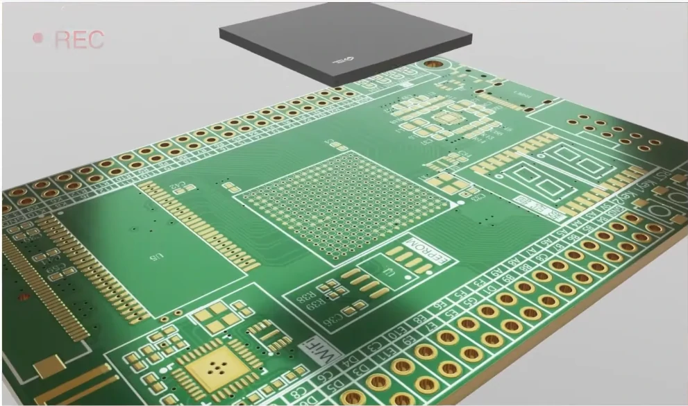
A BGA PCB is a printed circuit board designed for Ball Grid Array components. These packages support higher pin counts, smaller footprints, and better electrical performance than many traditional IC packages.
Today, BGA technology appears in processors, FPGAs, AI accelerators, networking equipment, automotive electronics, medical devices, and industrial control systems. Understanding BGA design and assembly helps engineers improve reliability, reduce manufacturing risks, and accelerate product development.
At Weller PCB, we regularly support customers developing complex BGA PCB projects for telecommunications, industrial automation, automotive electronics, and embedded systems. If you need fabrication or assembly support, you can request an instant PCBA quote.
What Is BGA? Ball Grid Array Basics

A typical BGA package contains a silicon die, a package substrate, solder balls, and an encapsulation layer. During reflow soldering, the solder balls melt and form both electrical and mechanical connections to the PCB.
Compared with QFP and QFN packages, BGA chips provide higher I/O density and shorter signal paths. These benefits make them ideal for high-performance applications such as processors, memory devices, FPGAs, GPUs, and networking ICs.
Many modern processor BGA devices contain hundreds or even thousands of connections. Traditional leaded packages cannot support this density efficiently. As products become smaller and faster, BGA technology continues to grow in importance.
| Package Type | Pin Density | Signal Performance | Typical Applications |
|---|---|---|---|
| BGA | Very High | Excellent | Processors, FPGA, AI |
| QFN | Medium | Good | Sensors, Controllers |
| QFP | Medium | Moderate | Industrial Electronics |
Advantages and Disadvantages of BGA Packages
BGA packages offer significant advantages for modern electronic products. However, they also introduce design and manufacturing challenges.
Advantages
The biggest advantage of BGA technology is higher connection density. Engineers can place more I/O connections in a smaller area. This feature helps reduce product size while increasing functionality.
BGA packages also provide better signal integrity. The shorter electrical path lowers inductance and resistance. High-speed interfaces such as DDR, PCIe, USB, and Ethernet benefit from this improvement.
Thermal performance is another advantage. Multiple solder balls create more heat transfer paths between the package and PCB. Better heat dissipation supports higher processing power.
Disadvantages
The main disadvantage is inspection difficulty. Solder joints sit beneath the package. Engineers cannot visually inspect them after assembly.
BGA packages also require more advanced PCB design techniques. Fine-pitch devices often need HDI technology, microvias, and via-in-pad structures. These requirements increase manufacturing complexity and cost.
| Advantages | Disadvantages |
|---|---|
| Higher I/O Density | More Difficult Inspection |
| Better Signal Integrity | Higher PCB Cost |
| Improved Thermal Performance | More Complex Routing |
| Smaller Footprint | More Difficult Rework |
What Is BGA in SMT?
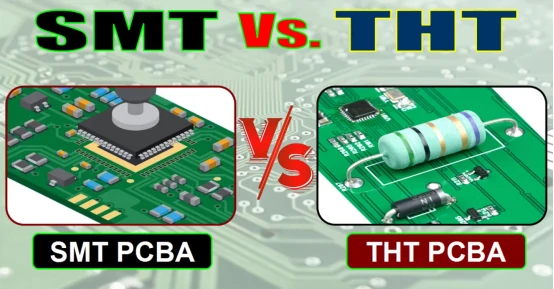
In SMT, or Surface Mount Technology, a BGA is a surface-mounted semiconductor package that uses solder balls instead of leads. Automated pick-and-place machines position the component onto solder paste deposited on the PCB.
The board then enters a reflow oven. Heat melts both the solder paste and solder balls. The solder forms strong electrical and mechanical connections.
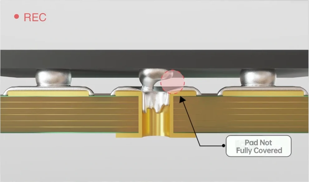
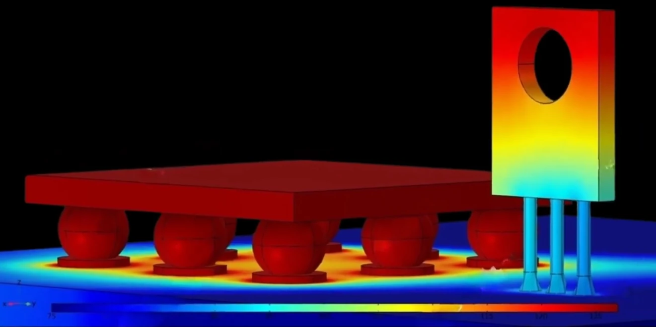
Compared with leaded packages, BGA assembly requires tighter process control. Small placement errors or improper reflow profiles can cause hidden defects such as voids, opens, and head-in-pillow failures.
SMT manufacturers widely use BGA packages in processors, communication modules, AI hardware, and advanced embedded systems because they offer higher performance and better miniaturization.
PGA vs BGA Processors
PGA and BGA are both processor packaging technologies. The primary difference is how the processor connects to the board.
PGA processors use physical pins inserted into a socket. BGA processors use solder balls attached directly to the PCB. PGA packages are easier to replace. BGA packages provide better electrical performance and smaller overall size.
| Feature | PGA | BGA |
|---|---|---|
| Connection Method | Pins and Socket | Solder Balls |
| Replaceable | Yes | No |
| Package Size | Larger | Smaller |
| Signal Integrity | Good | Better |
Modern laptops, embedded computers, networking devices, and AI systems commonly use BGA processors because they support higher density and better thermal management.
BGA PCB Design Guidelines
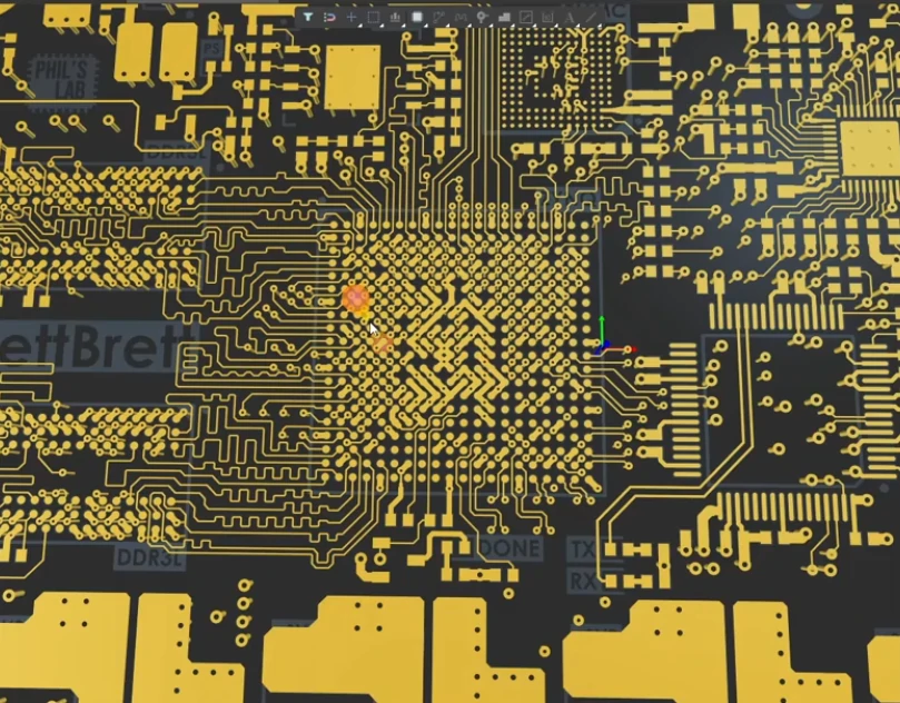
Successful BGA PCB design starts with footprint accuracy, stackup planning, impedance control, and manufacturability review. Engineers should not treat a BGA package as a normal SMT component. A dense ball grid array needs tighter control of pad geometry, solder mask clearance, via structure, escape routing, and power distribution.
Fine-pitch devices require special attention. A 0.8 mm pitch BGA may still support dog-bone fanout, but 0.65 mm, 0.5 mm, and 0.4 mm packages often need via-in-pad, laser microvias, HDI build-up layers, and tighter trace/space rules.
Many engineers review fine-pitch BGA routing guidelines before starting their designs.
BGA Footprint and Land Pattern Design
The footprint controls solder joint quality. Engineers should verify pad diameter, solder mask opening, ball pitch, courtyard clearance, and component keepout zones before layout. Most BGA designs use NSMD pads because the solder mask does not define the copper edge. This structure usually gives the solder joint better fatigue resistance during thermal cycling.
SMD pads may be useful when stronger pad anchoring is required, but they need tighter solder mask registration. Poor land pattern design can cause solder bridging, open joints, pad cratering, insufficient wetting, and head-in-pillow defects during assembly.
PCB Stackup Design
The stackup affects routing density, signal integrity, power integrity, EMI behavior, and manufacturability. A well-designed multilayer stackup gives high-speed signals a continuous reference plane and gives power rails a low-inductance return path. This is more reliable than routing dense BGA signals across split planes or weak ground structures.
For advanced projects, engineers should use a PCB stackup design guide to define signal layers, ground planes, power planes, prepreg thickness, core thickness, copper weight, dielectric constant, and controlled impedance targets before routing begins.
Controlled Impedance and Signal Integrity
Modern BGA chips often carry DDR, PCIe, USB4, Ethernet, LVDS, MIPI, RF, and SerDes signals. These interfaces need controlled impedance, length matching, differential pair spacing, return path continuity, and crosstalk control. Poor impedance design can create reflections, jitter, timing errors, eye-diagram closure, and intermittent system failures.
Engineers should calculate trace width, trace spacing, dielectric height, copper thickness, and reference plane distance early in the layout stage. Proper PCB trace impedance management improves signal quality and reduces redesign risk.
Power Distribution and Decoupling Strategy
High-performance BGA processors and FPGAs need stable power delivery. Designers should place decoupling capacitors close to power balls, use short via paths, and connect power and ground planes with low inductance. A weak power distribution network can cause voltage ripple, ground bounce, EMI problems, and random reset issues.
Good BGA PCB design balances routing density with power integrity. The layout should reserve enough space for bypass capacitors, thermal vias, current return paths, and test access. This planning makes the board easier to manufacture, assemble, inspect, and debug.
BGA PCB Board Layer Options
The required layer count depends on BGA pitch, routing complexity, signal speed, and power requirements.
A BGA 2 layer PCB may work for simple low-speed applications. However, most processor and FPGA designs require additional layers.
- BGA 4 Layer PCB: Suitable for simple embedded products.
- BGA 6 Layer PCB: Better routing flexibility and signal control.
- BGA 8 Layer PCB: Common for FPGA and communication devices.
- BGA 10 Layer PCB: Used for AI hardware, servers, and networking systems.
Higher layer counts provide more routing channels and stronger signal integrity. They also increase manufacturing cost.
BGA Fanout Routing and HDI Technology
Fanout routing moves signals away from BGA pads and into routing channels. This process becomes more difficult as BGA pitch decreases.
Dog-bone fanout works well for larger pitch devices such as 1.0 mm and 0.8 mm BGAs. Smaller pitches often require via-in-pad structures and microvias.
HDI technology plays an important role in modern BGA routing. Laser-drilled microvias and build-up layers support higher routing density and shorter signal paths.
Advanced processors often require any-layer HDI PCB structures to accommodate high pin counts and compact layouts.
HDI designs cost more than traditional multilayer PCBs. However, they enable smaller products, better performance, and more routing flexibility.
BGA Testing and Reliability
BGA testing is essential because solder joints are hidden beneath the package. Engineers cannot visually verify joint quality after assembly.
X-Ray Inspection
X-ray inspection helps detect voids, bridging, open circuits, and alignment problems. Automated X-ray Inspection (AXI) improves speed and consistency for production environments.
Electrical Testing
Manufacturers commonly use flying probe testing, ICT testing, and boundary scan testing. These methods verify electrical connectivity and help identify hidden faults.
Industry Standards
Reliable BGA products often follow IPC-7095 guidelines for BGA design and assembly. IPC-A-610 defines assembly acceptance criteria, while IPC-6012 establishes PCB qualification requirements.
JEDEC standards further support moisture sensitivity and reliability testing.
Choosing a BGA PCB Assembly Manufacturer
Selecting the right supplier affects quality, cost, and delivery performance. Not all PCB manufacturers have the capability to support advanced BGA projects.
A reliable supplier should provide:
- HDI PCB fabrication
- Fine-pitch BGA assembly
- Via-in-pad processing
- X-ray inspection
- IPC-compliant manufacturing
- Engineering support
Many OEM and ODM companies choose China BGA PCB assembly providers because they offer strong manufacturing capabilities and competitive pricing.
Weller PCB Manufacturing Company supports PCB fabrication, HDI PCB production, and BGA PCB assembly services for industrial, medical, telecommunications, automotive, and consumer electronics applications.
Conclusion
BGA technology has become a foundation of modern electronics. It enables smaller devices, higher performance, and greater functionality than many traditional package types.
Successful BGA projects require careful planning. Engineers must optimize footprints, stackups, routing strategies, assembly processes, and testing procedures. Procurement teams must select manufacturers with proven BGA experience and advanced inspection capabilities.
As processors continue to become faster and more complex, BGA PCB design and manufacturing will remain critical for future electronic products.
Frequently Asked Questions About BGA PCB
When does a BGA PCB require HDI technology?
HDI technology is usually recommended when BGA pitch reaches 0.65 mm or below. Fine-pitch devices often require microvias, via-in-pad structures, and higher routing density than conventional multilayer PCBs can provide.
What is the best PCB layer count for BGA designs?
The ideal layer count depends on pin count, routing complexity, and signal speed. Simple devices may work on 4-layer boards, while FPGA, processor, and networking applications commonly require 6, 8, or 10 layers.
Is X-ray inspection necessary for BGA assembly?
In most professional BGA assembly projects, X-ray inspection is strongly recommended. It helps detect hidden defects such as voids, insufficient solder, open joints, and alignment problems.
Why is BGA assembly more expensive than QFN assembly?
BGA assembly often requires tighter placement accuracy, advanced PCB fabrication, HDI structures, controlled reflow profiles, and specialized inspection equipment. These factors increase manufacturing complexity and cost.
How do I choose between BGA and QFN packages?
BGA packages work better for high pin counts, high-speed interfaces, and advanced processors. QFN packages are usually more cost-effective for simpler designs with lower connection requirements.


