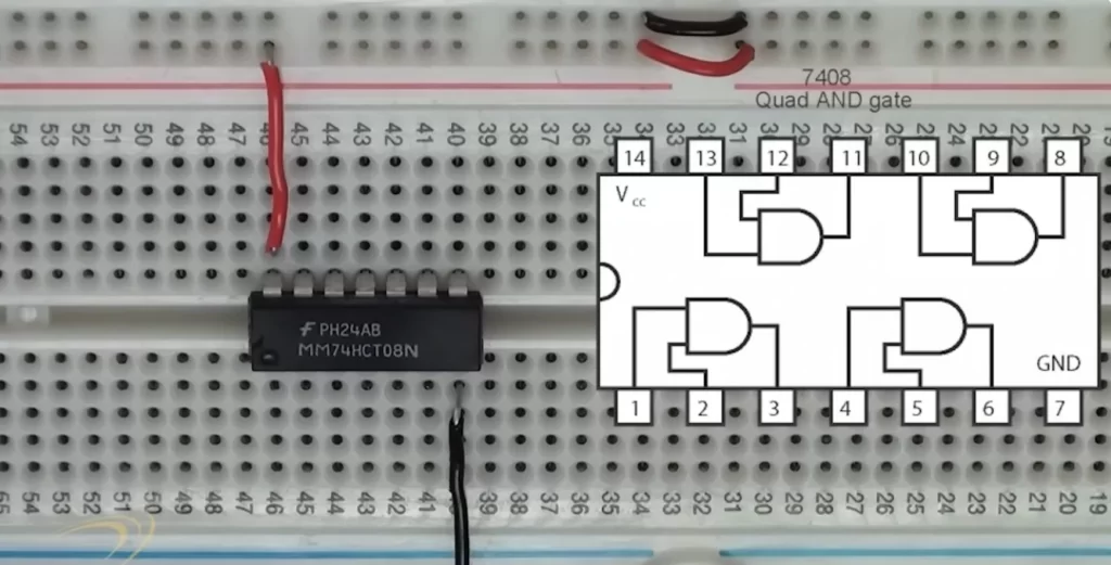
A dual inline package, or DIP, is an IC package with two parallel rows of pins for through-hole PCB mounting. It is larger than most SMT packages, but it is easier to test, replace, solder, and repair.
This guide explains DIP meaning, common package types, PCB design rules, assembly methods, advantages, limitations, and sourcing points. At Fast PCB Layout, we use this knowledge to help engineers improve PCB layout, assembly yield, and long-term product reliability.
What Is a Dual Inline Package?

A dual inline package is an electronic component package with a rectangular body and two parallel rows of electrical pins. Engineers also write it as dual in-line package, dual-in-line package, dual in line package, or D.I.P. The DIP full name is Dual Inline Package.
The package protects the semiconductor die and connects it to a printed circuit board. Each DIP pin passes through a plated hole. Solder forms a mechanical and electrical joint on the opposite side of the board. This through-hole structure is slower than SMT, but it is stronger and easier to inspect.
Many beginners ask, “what does DIP stand for in electronics?” “Dual” means two rows. “Inline” means the pins follow straight parallel lines. “Package” means the protective housing around the IC. This clear layout makes DIP electronics useful for learning, prototyping, repair, and low-volume production.
| Term | Meaning | Common Use |
|---|---|---|
| DIP | Dual Inline Package | Through-hole IC package |
| DIP IC | Integrated circuit in DIP form | Timers, op-amps, logic ICs |
| DIP socket | Socket for replaceable DIP chips | Testing and repair |
| DIP PCB | PCB designed for DIP components | Through-hole assembly |
The DIP format became popular because it made IC assembly easier and more repeatable. Wikipedia notes that the package style was developed at Fairchild R&D in 1964 and became widely used for early integrated circuits. You can review this reference on the dual in-line package.
DIP Package Structure and Types
A DIP package contains a semiconductor die, bond wires, a lead frame, an encapsulated body, and two rows of pins. The body may use plastic or ceramic material. The leads bend downward and fit into drilled PCB holes. This design gives the package better mechanical grip than many flat SMT packages.
The most common DIP pin pitch is 2.54 mm, or 0.1 inch. This spacing supports breadboards, test fixtures, and many DIP sockets. Common sizes include DIP8, DIP14, DIP16, DIP20, DIP28, DIP40, and PDIP-24.
PDIP Package
A PDIP package uses molded plastic. It is cheaper than ceramic and common in commercial electronics. Engineers use PDIP for timers, operational amplifiers, logic ICs, memory devices, and simple controllers. In most cases, when buyers say “DIP chip,” they mean a plastic DIP IC.
CDIP Package
A CDIP package uses ceramic material. It offers better sealing, higher thermal stability, and stronger environmental resistance. CDIP costs more than PDIP, but it suits aerospace, defense, laboratory, and harsh-environment electronics.
DIP Socket and DIP IC Socket
A DIP socket allows engineers to install a DIP IC without soldering the chip directly to the PCB. A DIP IC socket makes replacement easier. ZIF sockets reduce insertion force and work well in programming tools and test fixtures.
| Package Type | Main Feature | Typical Use |
|---|---|---|
| PDIP | Low-cost plastic body | Commercial ICs |
| CDIP | Ceramic body | High-reliability electronics |
| SPDIP | Shrink plastic DIP | Smaller through-hole designs |
| DIP socket | Replaceable IC mounting | Testing, repair, firmware work |
DIP vs SMT and Other IC Packages
DIP and SMT packages serve different design goals. DIP is easier to prototype, inspect, solder, and replace. SMT is smaller, faster to assemble, and better for dense electronics. A DIP component can offer stronger mechanical retention, while an SMT component gives higher board density.
DIP Package vs SMT Package
DIP needs drilled holes. SMT sits on surface pads. SMT supports faster automated production and lower unit cost at volume. DIP is more forgiving during hand assembly and rework. It is often better for labs, prototypes, education, repairable systems, and field maintenance.
PDIP vs DIP
PDIP is not separate from DIP. PDIP is one type of DIP. DIP is the larger category. PDIP means plastic dual inline package. CDIP means ceramic dual inline package. So, PDIP vs DIP is a subtype relationship, not a true package competition.
DIP vs SOIC, QFP, QFN, and BGA
SOIC is smaller than DIP and easier to automate. QFP supports more pins around four sides. QFN saves more space with no long external leads. BGA supports much higher pin counts under the package. DIP is simpler than all of them, but it cannot match their density.
| Feature | DIP Package | SMT Package |
|---|---|---|
| Board density | Lower | Higher |
| Repairability | Better | Moderate |
| Assembly speed | Slower | Faster |
| Prototype use | Easier | Harder without tools |
| High-frequency use | Weaker | Stronger |
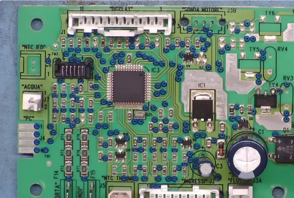
Mixed boards often combine DIP, SMT, connectors, and test points. Designers should review PCB layout guidelines for SMT assembly when they place different package styles on one board.
DIP PCB Design and Assembly Process

Good DIP design starts with the footprint. The footprint controls hole size, pad size, solder fill, and inspection quality. A weak footprint may pass schematic review but fail during assembly. A stronger footprint improves yield and lowers rework.
Hole Size, Pad Size, and Annular Ring
Engineers should choose a hole diameter that allows easy insertion and stable soldering. The plated through hole must match the lead size. The annular ring must remain wide enough after drilling tolerance. A larger annular ring is more forgiving, but it uses more PCB area.
Routing, Spacing, and DFM
DIP packages occupy more space than SMT parts. This larger footprint can make routing easier between pins, but it reduces available board area. Designers should leave enough clearance for inspection, repair tools, and solder flow. A DFM review before PCB manufacturing helps catch hole, spacing, polarity, and pin 1 marking issues early.
Soldering and Testing
DIP assembly may use manual insertion, automated insertion, wave soldering, or selective soldering. Wave soldering is faster for boards with many through-hole parts. Selective soldering is more precise for mixed SMT and DIP boards. Visual inspection, AOI, electrical testing, and functional testing help confirm final reliability.
Thermal design also matters. Power DIP devices may generate heat through leads and copper areas. Engineers should use copper pours, thermal reliefs, and correct spacing. The PCB thermal design guide explains how copper and layout choices improve heat spreading.
Advantages and Limitations of DIP Packages
DIP packages remain useful because they solve practical engineering problems. They are larger than SMT packages, but they are easier to handle. They are slower to assemble, but they are easier to inspect. They use more PCB area, but they support stronger mechanical joints.
Main Advantages
DIP components work well on breadboards. Engineers can test a DIP circuit before ordering a PCB. Technicians can replace a failed DIP IC with basic tools. Students can see the pin layout clearly. These features make DIP packages valuable for prototyping, education, repair, and low-volume production.
Main Limitations
DIP packages are not ideal for compact consumer devices. They need drilled holes and more board area. They support lower pin density than QFP, QFN, or BGA. Their longer leads can increase inductance and reduce high-speed performance. For dense IoT, RF, or mobile products, SMT is usually better.
Reliability Trade-Off
DIP through-hole joints can resist mechanical stress better than many small SMT joints. This helps industrial and serviceable products. However, DIP is not always more reliable in every case. The final result depends on solder quality, board design, component environment, and testing.
Applications and Sourcing Considerations
DIP packages still appear in many real products. They are less common in smartphones and ultra-compact products, but they remain useful in industrial electronics, education, test equipment, medical devices, and long-life systems. A larger package can be a weakness in consumer electronics, but it can be a strength in repairable equipment.
Common DIP Applications
Engineers use DIP IC package parts in microcontrollers, timers, operational amplifiers, optocouplers, EEPROMs, logic gates, drivers, and DIP memory devices. DIP8 packages often appear in op-amps and 555 timers. DIP28 and DIP40 packages often appear in older microcontrollers and development boards.
Sourcing and Obsolescence
Procurement teams should check lifecycle status before selecting DIP components. Some DIP integrated circuit parts remain common. Others are legacy or end-of-life devices. Counterfeit risk can be higher for older ICs. Teams should use approved suppliers and clear inspection rules to ensure authenticity of purchased electronic components.
Commercial Production Fit
DIP suits products that need repairability, socket replacement, strong joints, or lower prototype cost. SMT suits products that need compact size, lower unit cost, and faster assembly. The right package depends on production volume, product lifetime, field service needs, and supply chain risk.
How to Choose the Right DIP Package

Engineers should choose a DIP package by matching electrical needs, mechanical needs, production method, and service strategy. A package choice should not depend only on price. It should support the full product life cycle.
Check Pin Count and Footprint
Start with the pin count. Then confirm the package width, lead pitch, hole size, and PCB footprint. A DIP8 package needs less space than a PDIP-24. A wider package may improve routing but consume more PCB area.
Check Assembly Method
Small batches may use manual insertion. Larger batches may need automated insertion and wave soldering. Mixed SMT and DIP boards may need selective soldering. These process choices affect cost, lead time, and solder quality.
Check Reliability and Lifecycle
Review heat, vibration, humidity, availability, and repair needs. Industrial, medical, aerospace, and laboratory systems often value serviceability more than size. Compact IoT and consumer electronics usually value density and speed more than replacement.
Weller PCB Manufacturing Company supports prototype and production PCBA projects that include DIP components, SMT parts, connectors, and testing. For engineering support or pricing, you can request an instant quote for PCBA solutions.

Conclusion
The dual inline package remains useful because it solves problems that smaller packages do not solve as easily. It gives engineers better repairability, stronger solder joints, easier prototyping, and simpler inspection. SMT packages are faster and denser, but DIP packages are more practical when serviceability, education, low-volume production, or legacy support matters.
Future electronics will continue to use more SMT, QFN, and BGA packages. Still, DIP will not disappear from labs, industrial systems, test fixtures, and long-life equipment. Engineers should choose DIP when the product needs practical access and reliable through-hole strength. They should choose SMT when the product needs lower cost, smaller size, and higher production speed.
FAQ
What does DIP stand for in electronics?
What does DIP stand for in electronics?
DIP stands for Dual Inline Package. It describes an electronic package with two parallel rows of pins. These pins pass through holes in a PCB and are soldered on the opposite side.
What is the difference between a DIP package and a DIP socket?
What is the difference between a DIP package and a DIP socket?
What is the standard pin spacing of a DIP package?
What is the standard pin spacing of a DIP package?
The most common DIP pin spacing is 2.54 mm, or 0.1 inch. This spacing fits breadboards, sockets, and many through-hole PCB layouts. Some shrink DIP packages use tighter spacing.
Is DIP better than SMT?
Is DIP better than SMT?
DIP is better for prototyping, repair, education, and strong through-hole mounting. SMT is better for compact products, high-volume production, and high-density boards. The best choice depends on the product goal.
Are DIP packages still used today?
Are DIP packages still used today?
Yes. DIP packages are still used in development boards, industrial controllers, test equipment, medical devices, repairable systems, and legacy electronics where easy replacement and strong connections matter.