Most damaged PCBs do not fail for one random reason. Heat, moisture, vibration, poor soldering, electrical overload, and weak layout choices often create repeat problems.
Fast PCB Layout has helped manufacturers, OEMs, and product developers troubleshoot PCB failures and optimize board reliability through professional PCB design and layout services. Many repair issues can be traced back to preventable design decisions made during the early stages of board development.
This guide explains the 8 most common PCB repairs, how engineers diagnose them, how each repair works, and how better PCB layout practices can reduce future failures, lower maintenance costs, and improve long-term product performance.
What Is PCB Repair?
PCB repair is the process of restoring a damaged printed circuit board to working condition. A technician may repair copper traces, restore pads, replace failed components, remove solder bridges, clean corrosion, or fix damaged vias.
PCB repair is different from PCB rework. Rework usually corrects production defects before shipment. Repair usually restores a board that has already failed in use.
Many professional repairs follow IPC-7711/7721 repair guidance and IPC-A-610 assembly acceptability criteria. These standards help engineers achieve more consistent, safer, and more reliable results.
How Engineers Diagnose PCB Failures
Good repair starts with diagnosis. If you replace parts without finding the root cause, the same failure may return.
Visual Inspection
Engineers inspect the board for burn marks, cracked components, lifted pads, damaged traces, corrosion, and poor solder joints. A microscope often reveals smaller defects that normal vision misses.
Electrical and Thermal Testing
A multimeter checks continuity, resistance, voltage rails, and short circuits. Thermal cameras identify hot spots faster than touch-based inspection. This method is safer and more accurate for power electronics.
Functional Verification
After repair, engineers verify signals, power rails, startup behavior, and product function. A board is not truly repaired until it passes functional testing.
The 8 Most Common PCB Repairs

The 8 most common PCB repairs appear across consumer electronics, industrial controllers, automotive electronics, IoT devices, medical systems, and LED products. Some repairs are simple. Others need advanced equipment and trained technicians.
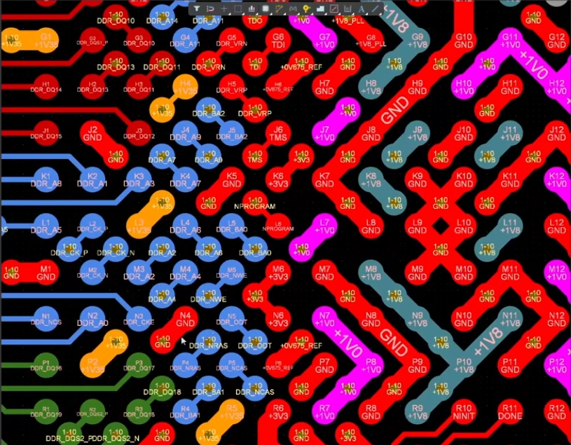
1. Broken PCB Trace Repair
A broken trace interrupts the copper pathway that carries power or signals. This failure can stop one circuit section or disable the whole board.
Common symptoms: power loss, missing signals, intermittent operation, or failed continuity tests.
Common causes: scratches, overcurrent, mechanical stress, board flexing, or heat damage. Thin traces fail faster than wider traces under high current.
Repair methods: technicians can use jumper wires, copper foil, conductive epoxy, or conductive ink. Copper foil usually provides lower resistance than conductive ink, so it is more reliable for higher-current circuits.
Prevention: use wider traces, better board support, and stronger current paths. Poor power and ground planes can increase heat and stress on copper routes.
2. Lifted or Missing Pad Repair
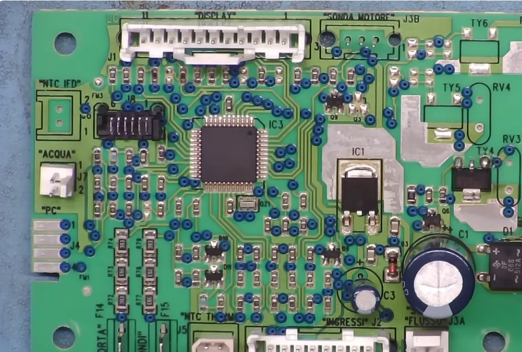
A PCB pad can detach from the laminate during excessive soldering or rough desoldering. This problem is common around connectors, SMT parts, and frequently replaced components.
Common symptoms: loose components, weak solder joints, missing electrical connection, or open circuits.
Common causes: high soldering temperature, long dwell time, weak pad adhesion, aggressive rework, or repeated thermal cycling.
Repair methods: a technician can install a replacement pad, bond it with epoxy, and reconnect it to the circuit. A jumper wire can also restore continuity when appearance matters less than function.
Prevention: use controlled heat and stronger pad geometry. Good PCB manufacturing design improves pad strength and assembly yield.
3. Cold Solder Joint Repair
A cold solder joint forms when solder does not bond correctly with the pad or component lead. It may look dull, rough, cracked, or uneven.
Common symptoms: unstable signals, intermittent operation, vibration-sensitive faults, or random power loss.
Common causes: low soldering temperature, dirty surfaces, weak flux activity, or movement during cooling.
Repair methods: technicians remove old solder, clean the area, apply fresh flux, and reflow the joint. A good joint looks smoother and forms a stronger connection.
Prevention: control solder temperature, flux quality, and reflow profiles. Better PCB design and assembly planning can reduce solder joint defects before production.
4. Solder Bridge Repair
A solder bridge creates an unwanted connection between two conductors. It usually causes a short circuit.
Common symptoms: excessive current draw, power supply protection, startup failure, heat near IC pins, or abnormal resistance readings.
Common causes: excess solder paste, poor stencil design, tight pad spacing, inaccurate placement, or insufficient solder mask clearance.
Repair methods: technicians remove the bridge with solder wick, flux, hot air, or a fine-tip soldering iron. They then check isolation with a multimeter.
Prevention: optimize stencil thickness, pad spacing, and SMT process control. Most solder bridges happen during the SMT assembly process.
5. Burned Component Replacement
Burned components often appear in power supplies, AC control boards, LED drivers, motor controllers, and industrial electronics.
Common symptoms: burn marks, cracked packages, bulging capacitors, blown fuses, failed MOSFETs, or a burnt smell.
Common causes: reverse polarity, surge voltage, overcurrent, short circuits, or poor thermal management.
Repair methods: technicians identify the failed part, test nearby components, clean carbonized areas, and install a part with the correct rating. They must confirm the root cause before power-up.
Prevention: improve derating, surge protection, copper width, and heat dissipation. Stronger design decisions reduce repeat component failures.
6. Corrosion and Water Damage Repair
Moisture can damage a PCB slowly. Corrosion increases resistance, creates leakage current, and weakens electrical connections.
Common symptoms: green or white residue, unstable connectors, random faults, leakage current, or failure after humidity exposure.
Common causes: water exposure, salt spray, chemical contamination, poor cleaning, or high humidity.
Repair methods: technicians use isopropyl alcohol, dedicated electronics cleaners, soft brushes, and sometimes ultrasonic cleaning. After cleaning, they repair damaged traces or replace corroded parts.
Prevention: use conformal coating, sealed enclosures, and cleaner assembly processes. Outdoor and industrial electronics need stronger protection than indoor consumer devices.
7. Via and Through-Hole Repair
Vias and plated through holes connect different PCB layers. When they fail, signals or power may lose connection between layers.
Common symptoms: layer-to-layer open circuits, failed through-hole components, vibration-related failure, or continuity on one side but not the other.
Common causes: barrel cracks, poor plating, thermal expansion, mechanical shock, or repeated flexing.
Repair methods: technicians may use wire stitching, eyelets, conductive repair materials, or jumper wires. Internal via damage is harder to restore than surface trace damage.
Prevention: choose proper drill sizes, plating quality, and via structure. Advanced boards using blind and buried vias need stronger design review because repair access is limited.
8. BGA and Advanced SMT Rework Repair
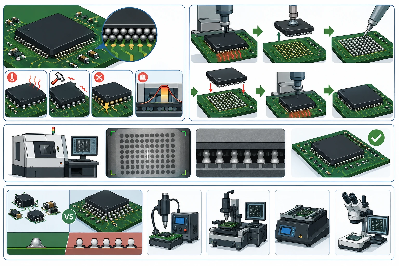
BGA repair is one of the most difficult PCB repairs because the solder joints sit under the package. You cannot fully inspect them with normal visual inspection.
Common symptoms: intermittent processor failure, memory faults, heat-related shutdown, failed X-ray inspection, or random startup problems.
Common causes: thermal cycling, board flex, solder fatigue, poor reflow profiles, or mechanical shock.
Repair methods: technicians use BGA rework stations, controlled thermal profiles, reballing tools, X-ray inspection, and functional testing. A basic soldering iron is not enough for reliable BGA repair.
Prevention: use balanced layout, proper thermal profiling, and good board support. Modern SMD components enable higher density, but they also require tighter process control.
Comparison Table of Common PCB Repairs
| Repair Type | Common Cause | Difficulty | Repairability |
|---|---|---|---|
| Broken Trace | Scratch, overcurrent, flexing | Low | High |
| Lifted Pad | Excessive heat | Medium | High |
| Cold Solder Joint | Poor soldering process | Low | High |
| Solder Bridge | Excess solder paste | Low | High |
| Burned Component | Electrical overload | Medium | Medium to High |
| Corrosion Damage | Moisture or chemicals | Medium | Medium |
| Via Damage | Thermal or mechanical stress | High | Medium |
| BGA Rework | Thermal cycling | Very High | Medium |
Why PCB Failures Happen
Most PCB failures come from five major sources. Heat accelerates component aging and solder fatigue. Electrical overload damages regulators, MOSFETs, fuses, and power paths. Moisture creates corrosion and leakage current.
Vibration affects automotive, aerospace, robotics, and industrial automation systems more severely than office electronics. Design deficiencies also matter. Undersized traces, weak power distribution, poor thermal paths, and tight spacing can create failures long after production.
Engineers who focus on first-pass PCB design success usually see fewer field failures and lower repair costs.

PCB Repair Tools and Cost Factors
Basic PCB repair tools include a temperature-controlled soldering station, multimeter, flux, solder wick, tweezers, isopropyl alcohol, and magnification equipment. The best soldering iron for PCB repairs should provide stable temperature control, fast heat recovery, fine tips, and ESD-safe operation.
Advanced repairs require more equipment. BGA repair may need a hot-air station, microscope, PCB repairing machine, BGA rework station, thermal camera, AOI system, or X-ray inspection.
| Cost Factor | Impact | Reason |
|---|---|---|
| Board Complexity | Higher cost | More circuits require more testing |
| Layer Count | Higher cost | Hidden layers are harder to inspect |
| BGA Components | Higher cost | Special equipment is required |
| Obsolete Parts | Higher cost | Sourcing takes longer |
| Testing Requirements | Higher cost | More verification increases labor |
PCB repairing cost is usually lower for broken traces and solder bridges. It is usually higher for BGA rework, corrosion spread, multilayer damage, and obsolete components.
How to Prevent Common PCB Repairs

The best repair is prevention. Better design creates fewer failures. Better manufacturing creates higher yield. Better testing catches defects before field use.
Improve PCB Design
Use proper trace width, stable power distribution, adequate clearance, and better component placement. Professional PCB layout services can identify electrical, thermal, and manufacturability risks before production.
Strengthen Thermal and Environmental Protection
Use thermal vias, wider copper, heat sinks, conformal coating, and sealed enclosures. Lower operating temperature usually creates longer product life.
Improve Manufacturing Control
AOI inspection, controlled solder paste deposition, stable reflow profiles, and functional testing reduce cold joints, solder bridges, and component failures. Fast PCB Layout supports engineering teams with PCB layout, design review, manufacturing planning, and assembly-related guidance.
Conclusion
The 8 most common PCB repairs include broken trace repair, lifted pad repair, cold solder joint repair, solder bridge removal, burned component replacement, corrosion repair, via repair, and BGA rework. These failures affect many products, from IoT devices and LED drivers to industrial controllers and automotive electronics.
A good repair does more than restore the damaged area. It also identifies why the failure happened. Root-cause analysis helps you avoid repeat failures. Better layout, stronger thermal design, cleaner assembly, and proper testing create more reliable boards.
If you are developing a new product, prevention is usually faster, lower-cost, and more reliable than field repair.
FAQ
1. What is the safest way to power a repaired PCB for the first time?
1. What is the safest way to power a repaired PCB for the first time?
Use a current-limited bench power supply when possible. Start with a lower current limit and monitor voltage, current, and heat. This approach can prevent secondary damage if a hidden short or wrong component remains on the board.
2. Can a cracked PCB still work?
2. Can a cracked PCB still work?
Yes, a cracked PCB may still work if no traces, vias, or inner layers are broken. However, cracks often worsen under vibration or heat. Engineers should inspect continuity across the crack before trusting the board in real use.
3. Why does a PCB fail again after repair?
3. Why does a PCB fail again after repair?
Repeat failure usually means the repair fixed the symptom but not the root cause. Common hidden causes include overcurrent, poor heat dissipation, weak power design, moisture exposure, or a damaged neighboring component.
4. Is it safe to repair medical or automotive PCBs?
4. Is it safe to repair medical or automotive PCBs?
Safety-critical PCBs require stricter control than hobby or consumer boards. Medical and automotive electronics may need traceability, functional validation, and compliance review. In many cases, replacement or certified repair is safer than informal repair.
5. How can PCB design reduce future repair needs?
5. How can PCB design reduce future repair needs?
Good PCB design reduces thermal stress, current overload, solder defects, and vibration damage. Wider traces, better grounding, proper spacing, thermal vias, and DFM review can lower failure risk before the board enters production.